Freely Available British and Irish Public Legal Information
[Home] [Databases] [World Law] [Multidatabase Search] [Help] [Feedback]
England and Wales High Court (Patents Court) Decisions
You are here: BAILII >> Databases >> England and Wales High Court (Patents Court) Decisions >> Nokia Technoloties OY v OnePlus Ltd Technology (Shenzhen) Co Ltd & Ors [2022] EWHC 2814 (Pat) (09 November 2022)
URL: http://www.bailii.org/ew/cases/EWHC/Patents/2022/2814.html
Cite as: [2022] EWHC 2814 (Pat)
[New search] [Printable PDF version] [Help]
Neutral Citation Number: [2022] EWHC 2814 (Pat)
Case No: HP-2021-000023
IN THE HIGH COURT OF JUSTICE
BUSINESS AND PROPERTY COURTS OF ENGLAND AND WALES
INTELLECTUAL PROPERTY LIST (ChD)
PATENTS COURT
The Rolls Building
7 Rolls Buildings
Fetter Lane
London EC4A 1NL
9 November 2022
Before:
MR. JUSTICE MEADE
- - - - - - - - - - - - - - - - - - - - -
Between:
|
|
NOKIA TECHNOLOGIES OY (a company incorporated under the laws of Finland) |
Claimant |
|
|
- and - |
|
|
|
(1) ONEPLUS LIMITED TECHNOLOGY (SHENZHEN) CO., LTD TELECOMMUNICATIONS CORP, LTD (4) OPPO MOBILE UK LTD |
Defendants |
- - - - - - - - - - - - - - - - - - - - -
- - - - - - - - - - - - - - - - - - - - -
MR. MICHAEL TAPPIN KC and MR. EDWARD CRONAN (instructed by Bird & Bird) for the Claimant
MR. GUY BURKILL KC and MR. DANIEL SELMI (instructed by Hogan Lovells International LLP) for the Defendants
Hearing dates: 20-22 and 26-27 September 2022
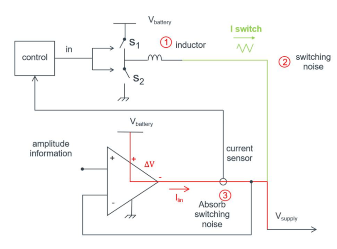
- - - - - - - - - - - - - - - - - - - - -
JUDGMENT
Remote hand-down: This judgment will be handed down remotely by circulation to the parties or their representatives by email and release to The National Archives. A copy of the judgment in final form as handed down should be available on The National Archives website shortly thereafter but can otherwise be obtained on request by email to the Judicial Office (press.enquiries@judiciary.uk).
Mr Justice Meade:
The common general knowledge. 8
Disputed CGK - power supplies. 8
Work on relevant systems around the priority date. 12
“for low-pass filtering the amplitude component”. 24
Claim 6 “feed-forward” path. 24
Further findings I was asked to make. 27
Conclusion on the infringement questions. 29
No a priori expectation when reading the prior art 31
Introduction
1. In this action, the Claimant (“Nokia”) alleges that the Defendants (together, “Oppo”) have infringed European Patent (UK) No. 3 716 560 B1 (“the Patent”) by the sale of certain mobile phones with 4G/LTE functionality (“the Oppo phones”); the trial was conducted by reference to three specimen devices. Oppo deny infringement and say that the Patent is invalid.
2. This action is part of a wider, global battle between Nokia and Oppo over the terms of a licence for Nokia’s patent portfolio. In a parallel action in the Patents Court, Nokia is deploying some standard-essential patents (“SEPs”), but the Patent is not alleged to be essential. It is what is sometimes called an “implementation” patent.
3. The alleged infringement arises from the operation of the chips inside Oppo phones. The chips are made by Qualcomm and their details are confidential. This has meant that Nokia has sought to prove infringement by doing experiments and by obtaining disclosure from Qualcomm in the US Courts using the procedure under 28 USC §1782 (“1782”).
4. During the proceedings, and in connection with the experiments, it emerged that software updates (“the Update”) to at least some Oppo phones meant that they no longer had the allegedly infringing functionality; this appeared to come as a surprise to both sides.
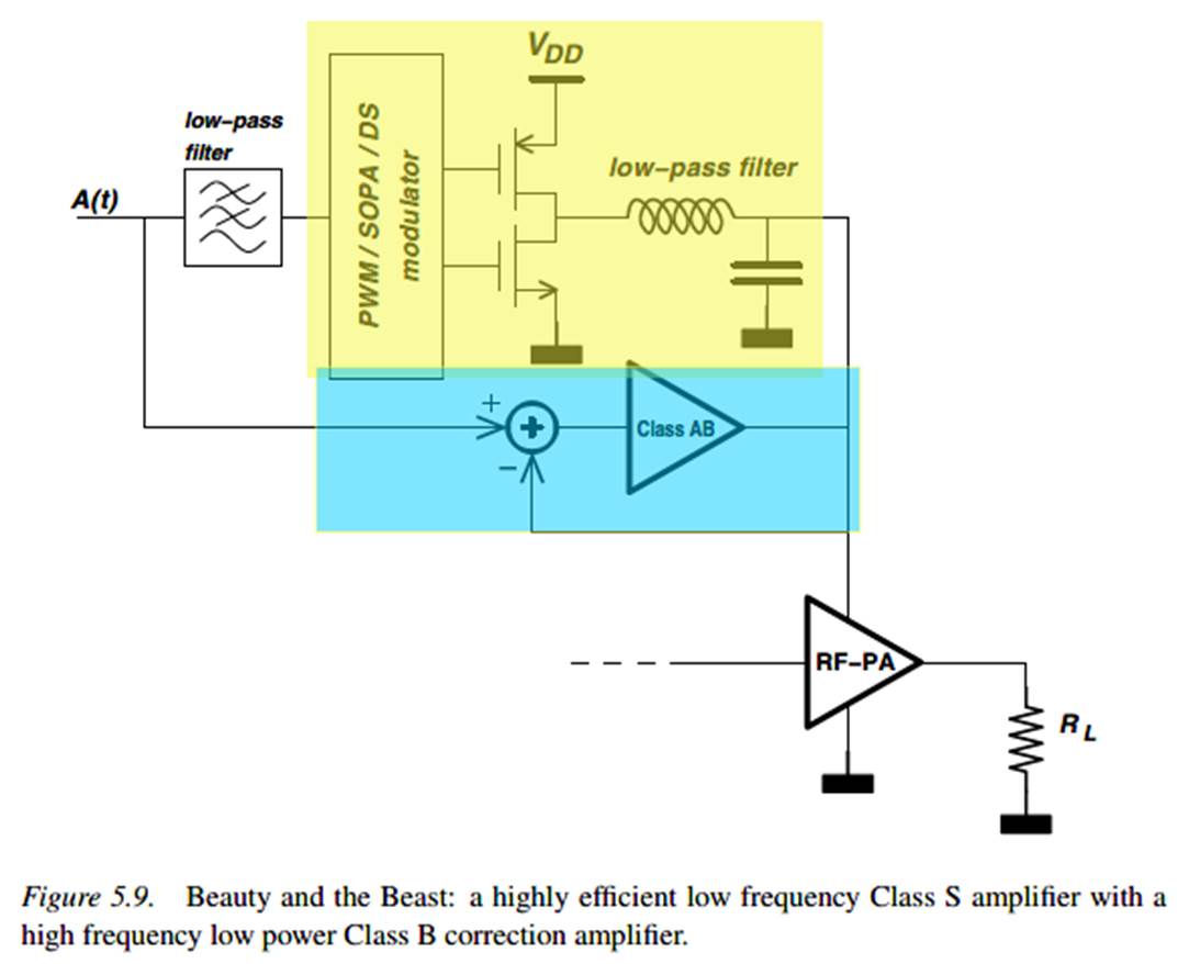
5. Nokia wanted to press ahead in relation to Oppo’s acts with phones prior to their having the Update. Nokia also said at interlocutory hearings that it had tested some more recent Oppo phones (“the Newer Oppo phones”) and that they retain the allegedly infringing functionality. Oppo has not accepted this and the Newer Oppo phones are not the subject of this trial. Nokia said that the situation with the Newer Oppo phones is another reason why this trial is necessary.
6. The situation with the Update demonstrates that it is possible to make and sell 4G/LTE mobile phones without infringing the Patent. That is not surprising given that the Patent is an implementation patent and not a SEP.
7. In that light, and generally, I have questioned during the course of these proceedings whether an action on a single implementation patent is a good use of resources or an efficient way to move the parties to a resolution of the overall issue of the terms of a new licence to Nokia’s portfolio, but I recognise that I do not have as good an appreciation of the dynamics between the parties as they do, and Nokia is clearly entitled to litigate what it regards as an invasion of a monopoly, even leaving aside the position with the Newer Oppo phones.
Conduct of the trial
8. The trial was conducted live in Court and there were no COVID issues.
9. Because of the highly confidential nature of the 1782 materials from Qualcomm, it was necessary to sit in private nearly all the time when discussing infringement. Although there were high level points that were not confidential and the experiments were not confidential (having been done by Nokia on sample devices bought, as I understand it, through normal sales channels) the practical reality was that they were too interwoven with the confidential materials.
10. I was satisfied that this was a proportionate way to proceed and drew an appropriate balance between Qualcomm’s justifiable concerns and open justice. Unlike many mobile phone cases there was little to no interest in the trial on the part of non-parties, and the result and principal reasons for it (which can be at a high level, as I explain below) will be made adequately open by this judgment.
11. I was assisted in drawing this balance by helpful submissions from Qualcomm. Qualcomm designated essentially everything from the 1782 process as highly confidential, with the result that access even for the parties has been severely restricted. I made it clear at an earlier hearing that that would require review because of the parties’ interest in knowing not only who has won, but why.
12. I also make clear, however, that Qualcomm’s position was one of a high level of caution at an early stage, when it was not at all apparent how much of the extensive materials given would be relevant and actually used in Court. As matters have progressed, very little need be used to understand the judgment. It boils down to one high level circuit diagram with all detail removed, of a circuit of a type which at a general level was well known, and even that is relevant only to a dependent claim not material to the overall result. I gave Qualcomm a further opportunity to make submissions on a draft of this judgment, prior to determining its public form for hand down, with the result that the entirety of this judgment is open. Had it been necessary to decide what, if anything, to put in a confidential part of this judgment then as well as the interests specific to this case, I would have been willing to take into account that third party disclosure procedures such as those under 1782 are a useful and necessary tool and it would be undesirable to deter compliance by acting without appropriate caution.
13. In its written closing submissions, Oppo accepted that in the light of the cross-examination of its expert and the totality of the materials (Nokia’s experiments and the Qualcomm 1782 documents) it could no longer dispute the presence in the Oppo phones without the Update of key features of claim 1. It qualified this concession in certain ways, notably by saying that it was on the basis of a particular construction, and it maintained a squeeze on a peripheral claim feature, but subject to those reservations this essentially amounted to admitting infringement. This has made the details of the experiments less relevant (although there may still be an argument about them on costs) and has also greatly reduced the need to refer to Qualcomm materials.
The issues
14. The issues are:
i) The scope of the common general knowledge (“CGK”). There are two major areas of disagreement.
ii) A number of points on claim interpretation relevant to validity over the prior art and to the infringement arguments.
iii) Infringement, there being no remaining dispute of fact material to the overall result. There is however an issue over whether I should make certain additional factual findings and an issue over dependent claim 6.
iv) Validity over three pieces of prior art (the attacks are all of obviousness, anticipation is not alleged):
a) US patent application US2006/0178119 A1, “Jarvinen”.
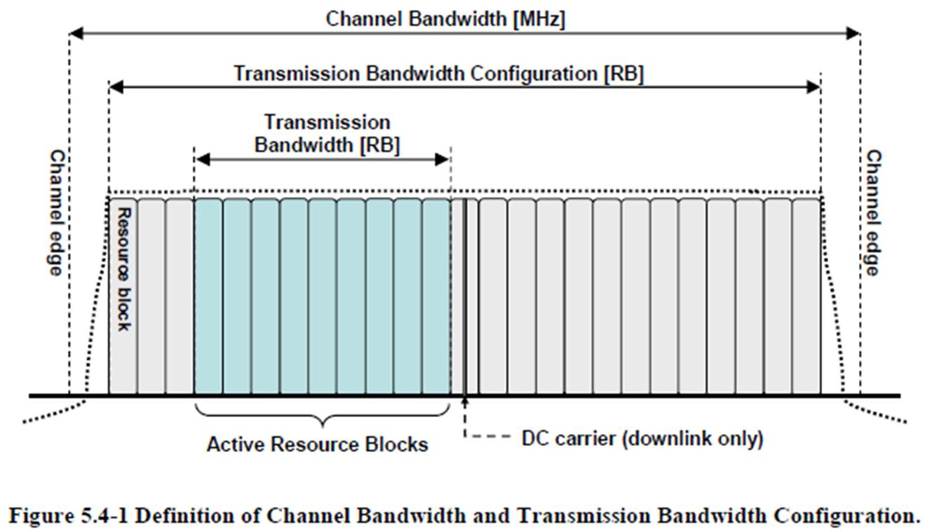
b) European Patent Application EP 1 598 943 A1, “Arayashiki”.
c) An article from the IEEE 2004 Custom Integrated Circuits Conference “Hadjichristos”.
v) A sufficiency squeeze on obviousness.
vi) The allowability of two amendments to the Patent proposed by Nokia.
15. There was one issue that was central to the validity arguments. That was whether it was obvious in the light of what was generally known about LTE to conceive of and put into practice the main idea of claim 1 of the Patent. I have reached the view that Nokia is right about this point, which applied with similar logic and force to all the prior art citations. There are other more minor points on each citation, but Nokia’s success on this one means that all the prior art attacks fail.
16. The result of that, as I shall go on to identify, is that the allowability of the amendments to the Patent do not matter because they were both made to distance its claims from the prior art. So I am going to deal with those points only briefly in case on any appeal my decision on obviousness is overturned.
17. Also, Nokia maintained the independent validity of claim 6. This raised additional issues of claim interpretation, infringement, and obviousness. Having won on claim 1, Nokia does not need claim 6, so I will deal with that briefly as well.
The witnesses
18. Each side called one expert. Nokia’s expert was Prof Bram Nauta. Oppo’s expert was Dr Jan Crols. Each had very good and relevant technical experience, as well as academic exposure to the art. Minor points were made about which had greater industry experience and which had done work most approximating to the specific task in this case (designing an LTE transmitter in 2007) but the points were rightly not pressed with any enthusiasm and I did not find them of assistance.
19. However, each side criticised the other’s expert in respect of other matters which they said were more important.
20. Oppo criticised Prof Nauta for not having in mind the right skilled team, and in particular not envisioning them as knowing enough, indeed not much at all, about the relevant aspects of LTE at the priority date. I agree with this criticism; Prof Nauta’s first report envisaged a skilled team with only the most minimal idea of the power requirements for an LTE transmitter and minimal conception, perhaps even none, of RBs and their intended uses, including dynamic allocation and impact on bandwidth utilisation. This was all the stranger given that he had had, as Oppo said, to acquaint himself with those matters for the purposes of Nokia’s infringement analysis, with which he was involved from early in the case.
21. Although I accept this criticism, there are two major caveats to it.
22. The first is that I think it was most probably a result of the way he was instructed or because he misunderstood the concept of the skilled team, and I would reject any assertion that his misconception in this regard reflected on his independence or integrity. He struck me as very honest and straightforward.
23. The second caveat is that the error was very strongly manifest in his first report, but dwindled in significance in his later reports and in his oral evidence. By the time he was giving me his opinions I am confident that he was factoring in the possibility of the skilled team knowing a lot more about LTE and the reasoning that would follow. So although this criticism must be borne in mind, and I do so, it was a long way from fatally undermining his evidence and I reject Oppo’s contention to that effect.
24. The other criticism pressed hard against Prof Nauta was that (Oppo said) he had thought it inventive for a mobile’s hardware set-up to be affected by base station commands; Oppo pointed out that e.g. multimode phones could be directed to change modulation by the base station and that this was CGK, as Prof Nauta accepted. I do not think there was anything in this criticism. I do not consider that Prof Nauta ever squarely said that the skilled team would be unaware through CGK of any situation where a mobile’s hardware setup was changed on the direction of the network, but rather he said he thought the kind of change required by the claims of the Patent would not be thought of without invention. Indeed in the key passage relied on by Oppo (T2/112) he accepted that the multimode situation would be CGK, but did not accept that his evidence was based on the assumption “that the skilled person would be unfamiliar with the basic principle of mobile telephony that the base station controls the mobile.” He just said that the skilled team would work to the standards.
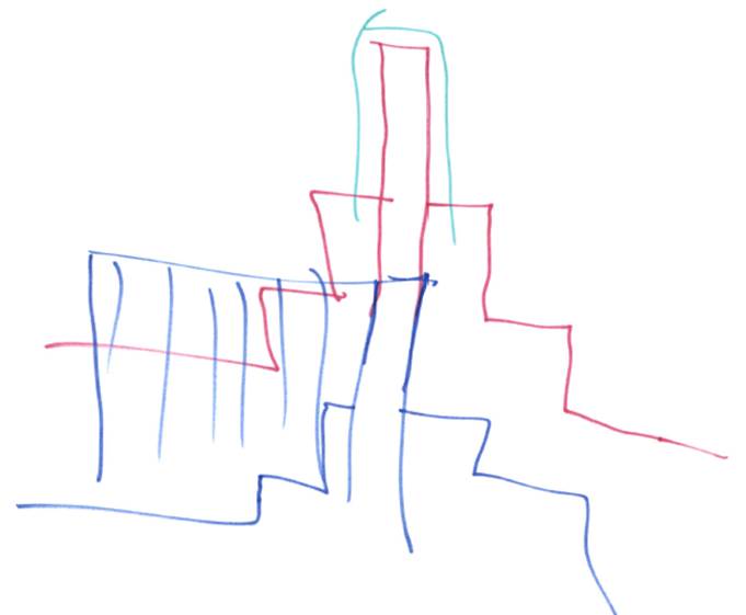
25. As to Dr Crols, Nokia’s criticism of him was not personal. They pointed out that he was inventive but (correctly) accepted that that was not in itself a problem as long as the expert put himself in the position of the skilled team. Nokia said that he failed at the latter stage.
26. Nokia pointed out that Dr Crols did not see Jarvinen or Hadjichristos until after he saw the Patent, and that although he saw Arayashiki about a week before he saw the Patent, it was not until later that he saw the LTE standards, whose combination with Arayashiki, and the cited prior art generally, was key to Oppo’s case.
27. As has been observed in other cases, it is better if an expert giving evidence that a patent is obvious sees the prior art first, but this cannot always be achieved. If it is not, there is a risk of hindsight and the expert has to guard against it, and think about how to avoid it. There may or may not be some positive way of showing that the expert has been able to put prior knowledge of the invention to one side (giving examples, showing their reasoning with special care) but often they will simply have to make clear that they were so instructed and tried their best. In the present case, I accept that Dr Crols was so instructed, and did try.
28. That does not mean that he succeeded, however. I find that he did not. I thought his evidence was heavily burdened with hindsight. The reasons for this will make fuller sense as I go through the issues below, but in outline:
i) His postulating the “1 RB v 100 RB” issue was central to his thinking but its origins were inadequately articulated and not shown to come from the CGK.
ii) His focus on individual parts of the circuitry of the prior art showed a treatment which artificially homed in on those most relevant to the invention of the Patent without regard to whether they would have been of any particular interest to the skilled team.
iii) The prior art citations are not generally directed to the problem addressed by the Patent but Dr Crols did not really explain why nonetheless they would be of interest.
29. None of this reflects on Dr Crols’ integrity or independence. It is not an easy job to give evidence about obviousness without letting hindsight in and it is not a personal criticism of him that he did not cope with it well.
30. Overall therefore I thought Prof Nauta was a significantly better guide to the thinking of the ordinary uninventive skilled team, and I reach that conclusion while making due allowance for the shortcomings of his evidence in relation to LTE.
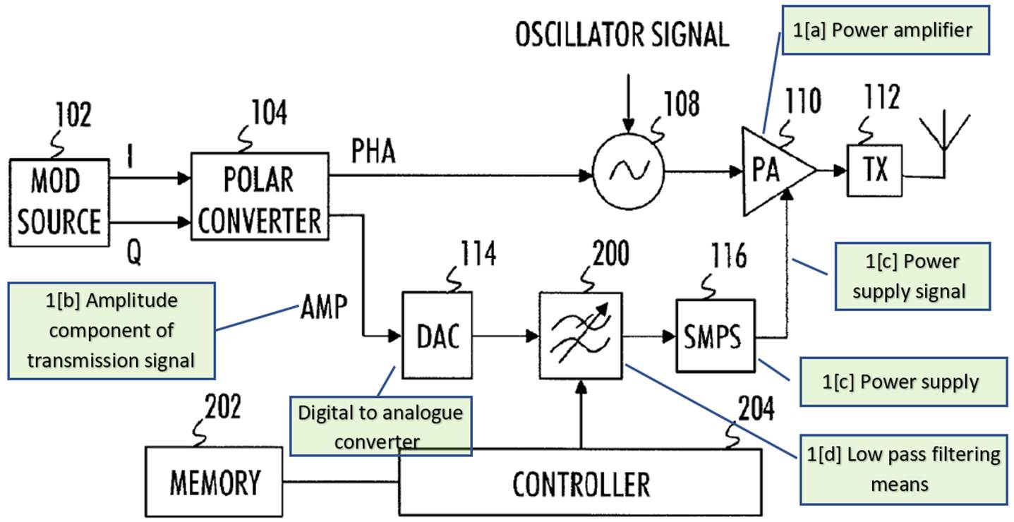
31. During the interlocutory stages of this action, a witness statement was provided from a Mr Mirea of Qualcomm. At a further interlocutory hearing I gave permission for Nokia to call him to be cross-examined. His statement spoke to certain changes made to the Qualcomm software in question and the reasons for those changes. As matters turned out, Nokia took the pragmatic view that it was unnecessary to cross examine him to find out how the chips in question actually worked. I found the explanations contained in his statement difficult to follow. This was not, I stress, because I thought he was lacking in candour, but because of the complexities of what he was trying to address in a very short statement. The lack of cross examination does not affect my ability to understand the necessary evidence relevant to whether or not there is infringement but it does mean that not every point of fine detail has been explored and I take that into account when I come to decide what findings I should make on the facts as to infringement.
The skilled addressee
32. There was little dispute about the identity of the skilled team.
33. Oppo said the skilled team would consist of (a) an RF designer who would design the front end radio transmitter, their task being to design and test the hardware; and (b) a systems architect who would make decisions about the overall design and architecture of the transmitter, including the baseband circuitry and the front end. Nokia, on the other hand, saw things in slightly less black and white terms but did not disagree in the end with the overall coverage of the skilled team.
34. In any event, as I have said each party called one expert, each of whom was able to speak to these areas of expertise.
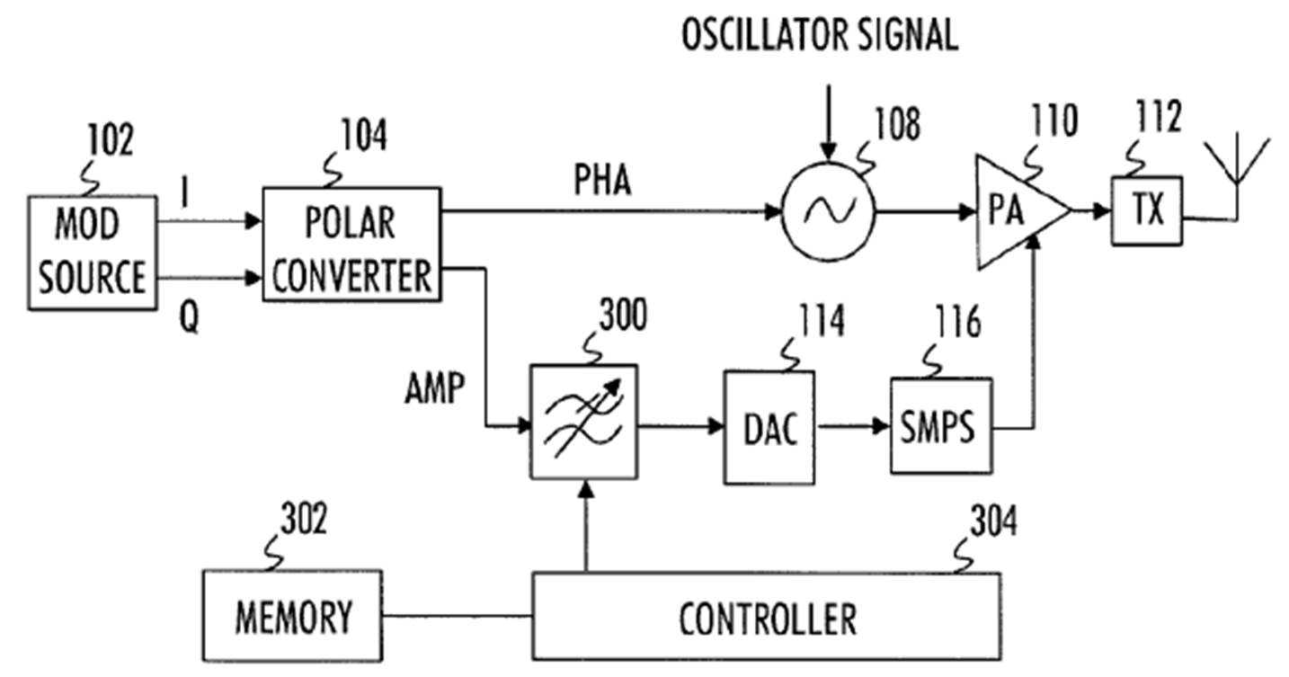
35. I record that Nokia accepted that it was legitimate to consider a skilled team seeking to design a transmitter for LTE. That makes sense because the Patent is primarily addressed to a problem which would arise in LTE, although its claims are not so limited. I would have thought it more natural to build interest in LTE into the characteristics of the skilled team. The parties instead addressed it in connection with CGK, but I do not think this made any difference.
The common general knowledge
36. In keeping with current practice in the Patents Court, there was a joint document which showed the CGK that was agreed (the “ASCGK”) and another identifying what was in dispute. There were four listed issues of CGK in dispute. One dropped out of the picture altogether and two others naturally go together. So I deal with the disputed CGK under two headings below.
Agreed CGK
37. The ASCGK forms the Schedule to this judgment (I also quote from it a little below). It was extremely helpful and I am very grateful. It contains quite a lot of basic explanation that is not specific to this action but is necessary to understanding the material that is of more direct relevance. I invite readers of this judgment to go through it, and then resume this judgment here. Those unfamiliar with this field may find it useful to read the whole, while those who already have a general understanding of radio transmission, modulation, transmitter components and amplifiers will need to read less; for them, the parts that I consider of particular importance and/or usefulness, and/or on which the parties concentrated their submissions, are paragraphs 37-38, 54-56, 72-77 and 93-96. This indication is for the assistance of readers of this judgment and does not mean that I have not had regard to the whole document; I have.
Disputed CGK - power supplies
38. There was no dispute that the skilled team would know about power supplies which combined a linear power supply and an SMPS. The issue is over which kinds.
39. Nokia says that a set-up referred to as “Wang” was CGK. This combined a linear power supply to which a current sensor was applied, with an SMPS. Putting it rather crudely, the SMPS did the heavy lifting and the linear amplifier provided the fine detail. Their combination in this particular way meant that there was no need for a capacitor at the output of the SMPS (only an inductor) and so no low pass filter (“LPF”).
40. The following is one of a number of depictions of a Wang system:
41. Nokia says that this is the sort of power supply that would be used for the challenges presented by the high bandwidth requirements of LTE. If the skilled team’s CGK options were limited to Wang-type systems for LTE then Nokia’s position would be very strong because there would be no ready possibility of an adjustable LPF.
42. There was no serious dispute on the evidence that Wang was CGK. It was the subject of a number of notable publications in 2005/6/7 from well known groups and which Prof Nauta said made a major impact in the art. Dr Crols essentially accepted this.
43. On the evidence, I also find that there were variants of Wang; it was not just a single idea. For example, there was a publication called Kwak which was a development, and I say a little more about it below.
44. Whether Kwak was CGK was not rigorously gone into at trial, and certainly not to the extent that Wang and Reynaert (see below) were canvassed. But Prof Nauta said that it was “well known” in the same way as Wang and I therefore conclude that it was CGK. That does not mean that every detail of it was, though, and in closing Oppo sought to rely on aspects of it that were not explored in cross-examination. That was not legitimate.
45. Oppo did not agree that the CGK was limited to Wang (and Kwak). There were two main strands to its position:
i) It said that it was CGK that an SMPS alone could be used in a way suitable for the high bandwidths of LTE. It said that there were improvements to the basic SMPS set-ups that allowed this and that they were CGK.
ii) It said that a set-up referred to as Reynaert or “Beauty and the Beast” was CGK. As with Wang, there were variants.
46. Either of these would incorporate an LPF and therefore be compatible with implementing the basic idea of the Patent (if the skilled addressee thought of it).
47. I will deal with these in turn.
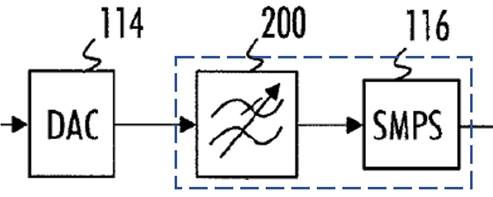
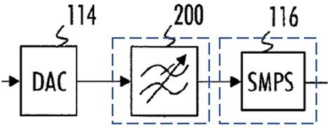
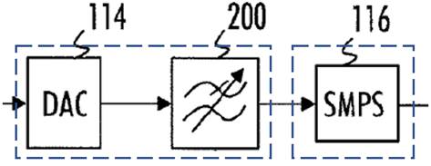
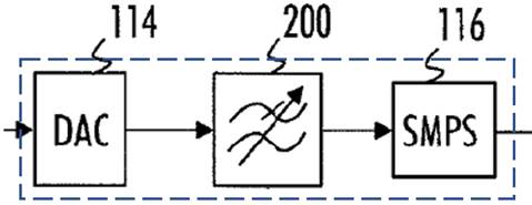
SMPS only
48. Oppo did not seriously dispute that simply taking the well known kind of SMPS alone and using it for a high bandwidth situation would have been seen as problematic.
49. But Oppo said that the art had developed ways to address this. In particular, it relied on a publication called Pinon, and a Texas Instruments patent application.
50. Pinon was published after the priority date and was suitable for WCDMA, a significantly lower bandwidth than LTE. It was not shown to have had wide circulation.
51. Texas Instruments’ application was filed before the priority date of the Patent but not published until afterwards. It is quite possible that it had at least a partial solution to the problem of using an SMPS-only supply for wide bandwidth but it was clearly not well known before the priority date and involved making an invention.
52. I conclude that neither Pinon nor Texas Instruments helps Oppo on this point and it was not part of the CGK to use an SMPS-only supply for wide bandwidth situations such as would arise with LTE.
53. In arguing that these kinds of solutions for SMPS-only supplies must be CGK, Oppo pointed out that its sufficiency squeeze had forced Nokia to abandon any non-enablement points over the prior art, and further that the Patent says that power supplies “comprising” an SMPS could be used with its invention. I will briefly digress from the CGK to address that; it fits naturally here.
54. Nokia’s answer, which I accept, was in two parts. The first was that it was not saying that the prior art was not enabled for what it specifically taught. I accept that, although it is only a partial answer because this kind of “shepherding” squeeze is directed to constraining the patentee from relying on lack of enablement or implementation obstacles as an answer to obvious developments of the prior art: the patentee cannot rely for inventive step on implementation problems not addressed by the patent’s teaching.
55. Nokia’s second answer was that the invention of the Patent is indifferent to the details of the power supply and lies in the idea of programmable variation of the cut-off frequency of a filter; it does not promise that every power supply would be enabled and does not need to. I agree with this. Furthermore, adequate power supplies comprising an SMPS were part of the CGK, in the form of Wang. I do, however, consider that arguing that the Patent is indifferent to the precise form of power supply is inconsistent with, or at least in tension with, Nokia’s contention on claim interpretation that the LC filter at the output of an SMPS does not satisfy the requirements of claim 1 of the Patent. But I reject that contention below.
Reynaert
56. This was another combination supply. The following is a schematic taken from one of Dr Crols’ reports:
57. This has a yellow “beast” SMPS which does the heavy work and a blue “beauty” linear supply. It has an LC filter at the output of the SMPS and a “content splitter” LPF at the input. It also differs from Wang in that it does not have the current-sensing control of the SMPS by the linear supply.
58. In my view Reynaert was not shown to be CGK:
i) It was first to be found in a book by Reynaert. Superficially this sounds like a promising start for CGK, however the book in question was not a standard text, but rather a reformatting of Dr Reynaert’s PhD thesis.
ii) This was, on the evidence, quite a common approach by publishers and there was nothing sinister about it, but such books had very limited circulation, quite possibly only a few hundred.
iii) Prof Nauta had never seen it before.
iv) If the skilled team would, notionally, have seen the Reynaert book they would not be told that the combined supply was an established approach. Reynaert does not say that it had been put into practice.
v) As the case progressed, Oppo’s advisers found a later publication called Yousefzadeh which it was said showed a simulation of a Reynaert circuit, and Dr Crols also pointed to a publication called Raab which Prof Nauta had exhibited. Neither of these rose to the level of showing general acceptance or even near it in my view. Prof Nauta said they would not work and although Dr Crols did not agree, I find that skilled readers would at best have been unclear as to their reliability.
59. These were the main points and there were other more minor ones. Taken as a whole, Reynaert was neither well known nor, even to the extent known, generally accepted as a good basis for future action.
60. In closing submissions, Oppo rather over-generalised the Wang/Reynaert issue, I felt. What I mean is that Oppo argued that parallel combinations of linear and switching supplies were CGK (viz. Wang, for example), that splitting them into sub-types was unnecessary, and that since that broad class was CGK, Reynaert was. This was a rather obvious fallacy: “some combination supplies were CGK, Reynaert is a combination, therefore Reynaert was CGK”. It is a fallacy because it omits to take account of the possibility that some but not all combinations were CGK, as indeed I have found to be the case.
61. Oppo even went so far as to submit that since some combination supplies were CGK, the differing details of their circuitry was “secondary”. In the context of this case, that was not so. There was an obvious importance to the difference between Wang and Reynaert in relation to the use of an LPF.
Work on relevant systems around the priority date
62. Nokia relied on various publications to show what it said was the direction of travel in the art. This was partly relevant to power supplies and partly relevant to the more general position in relation to variable LPFs. This is not CGK as such, not least because some of the materials relied on are post-priority, but this is a convenient place to deal with it.
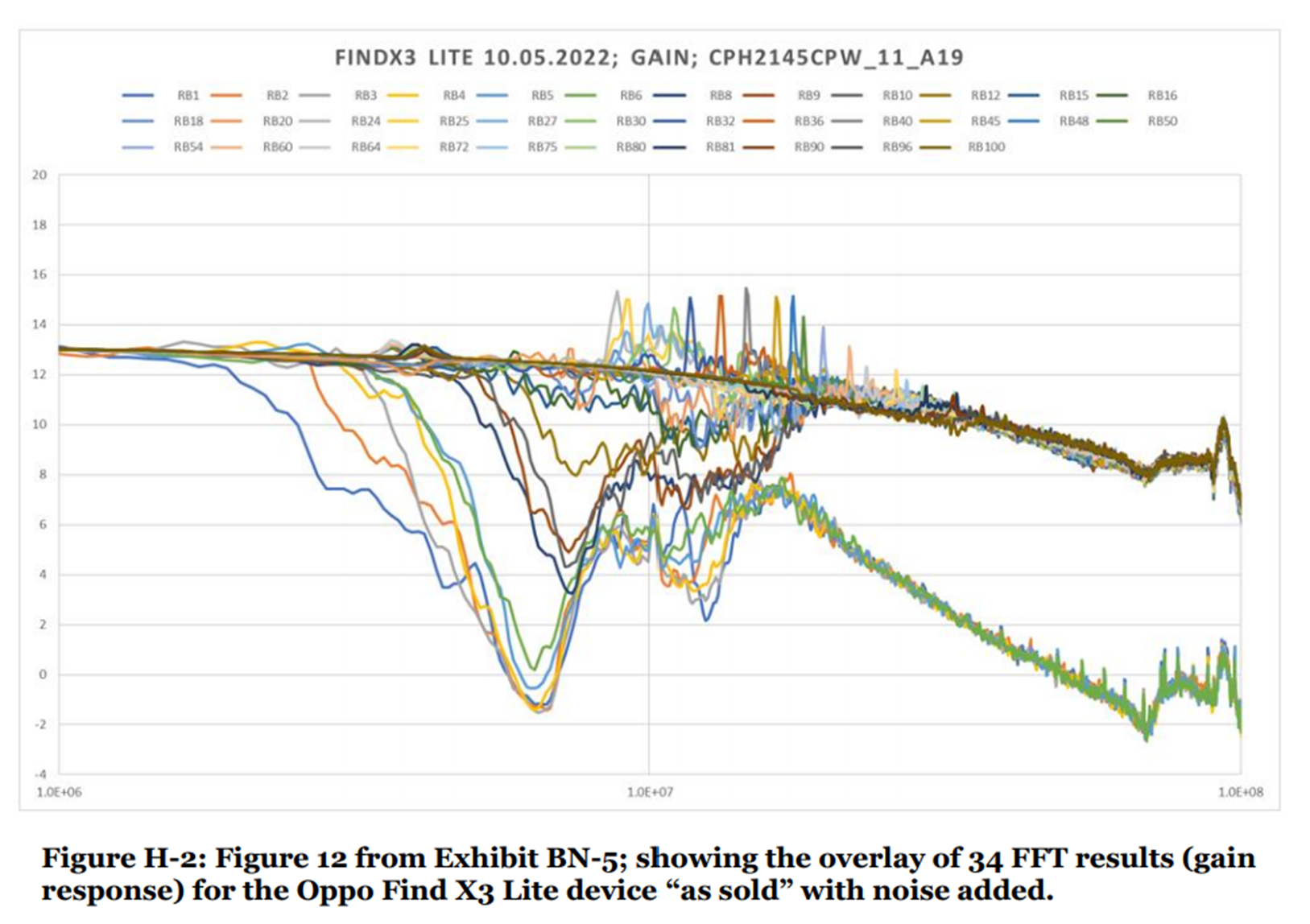
63. Thus, Wang-based systems were intended originally for use in WLAN, with a view also to WiMax, and could transmit with a 20 MHz bandwidth (very similar to LTE). Later work by Lie and by Kim in fact deployed it for WiMax. In due course, Kim also used it for an LTE transmitter.
64. This is consistent with Nokia’s case that Wang would have been the way to go for power supply in LTE: I cannot be confident that it presents the complete picture and other groups may have taken different approaches. But if they had published such work then I think Oppo would have found it. So this provides some support for Nokia’s position.
65. Nokia also pointed out that there was no sign in the literature of the use of LPFs whose frequency was tunable so as to deal with the challenges of wide band systems, including variable bandwidth systems (it accepted that LPFs tunable to address production variance were CGK), either before or for some years after the priority date. So it pointed to transmitter designs for WLAN, WiMax, and LTE referred to above (Lie, Kim), and another called Hassan (2011).
66. As with the power supply point, it is not possible to be confident that this is the whole picture, and I do not accept Nokia’s point that if there had been the use of a tunable LPF it would necessarily have been published. But, again, this provides a sense of real-world consistency to Nokia’s case.
Disputed CGK - LTE
67. To set the context for the disputed CGK I will begin by quoting the ASCGK on matters not in dispute as they relate to LTE:
“95. The LTE standard was still under development in December 2007. Not all of the transmitter performance requirements had been standardised. It had been decided that LTE would use OFDMA in the downlink and SC-FDMA in the uplink, with QPSK, 16QAM and (for the uplink, eventually) 64QAM modulation schemes, which would require a transmitter with high modulation accuracy (and therefore low EVM - for example it was likely that 12.5% would be required for 16QAM) and high PAPR. There were to be a number of different transmission bands at different carrier frequencies, with different bandwidths, including 5, 10, 15 and 20 MHz (a substantial increase over the 3.84 MHz bandwidth of WCDMA). The maximum output power requirements were likely to be in the range of +25 to +27 dBm (i.e. about 0.5 W). The ACLR requirements would depend on the bandwidth of the transmission band, but for a 20 MHz bandwidth it was likely that the requirement would be for a -30 dB difference between the power in the central 18 MHz of the transmission band and the power in the 25 MHz above or below the transmission band. (Nauta 1 §192, Crols 2 §5.49)
96. In LTE a resource block is the smallest unit of physical resources. The bandwidth of a single RB is 180kHz, made up of 12 subcarriers (each with a bandwidth of 15 kHz) in the frequency domain and 1 slot (0.5 ms) in the time domain. (Nauta 1 §193; Crols 1 §6.86)”
68. This represents the bare bones of LTE relevant to transmitter design. Of course, it would suit Nokia’s case if the CGK were so limited because although the ASCGK recognises the existence of resource blocks, it does not say anything about their being variable, or the nature of that variability.
69. Nokia’s position on this was unrealistic. It is tied in to the issue of the skilled addressee that I have mentioned above. Even if the transmitter designer in the skilled team were not themselves familiar with the parts of LTE relevant to resource block allocation they would need to find out from someone who knew about standards. It would be incompetent not to do this to the level necessary to the task of designing a transmitter, and, as Oppo said, if it were not done the team would “make an expensive mistake”.
70. I hold therefore that a competent skilled team would find out the following additional matters about LTE from the standards (taken largely from Oppo’s opening submissions, based on Dr Crols’ report).
71. First, that the relevant standard documents were:
i) TS 25.814 v.7.1.0 produced in September 2006 and uploaded onto the 3GPP website on 13 October 2006.
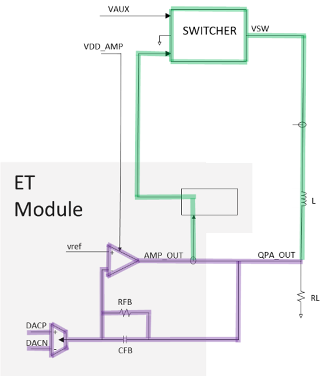
ii) TS 36.211 v.8.0.0 produced in September 2007 and uploaded onto the 3GPP website on 27 September 2007.
iii) TS 36.101 v.1.0.0 produced in December 2007 and uploaded onto the 3GPP website on 11 December 2007.
72. Not all of their contents would be CGK but the skilled team would know where to find them and how to identify the key contents.
73. Second, TS 36.101 defined the following at its section 3.
Transmission bandwidth: Bandwidth of an instantaneous transmission from a UE or BS, measured in Resource Block units.
74. It also provided a helpful illustration at 5.4.2:
75. Third, the following points:
i) LTE adopted a variable signal bandwidth for downlink and for uplink transmissions (see TS 36.101 at section 5.4.2).
ii) This was the first time that a variable channel bandwidth had been used for a wireless mobile telecommunication standard.
iii) The structure of the uplink and downlink physical channels and in particular the definition of "resource blocks" or RBs was defined (see TS 36.211 at sections 5.2.3 and 6.2.3.
iv) The channel arrangement, the number of channel bandwidths, and the maximum number of RBs available to be allocated to a terminal in each was defined (see TS 36.101 at section 5.4).
v) The bandwidth used by a terminal was determined by the number of RBs allocated to that terminal, not by the channel bandwidth (see TS 36.101 at section 5.4).
vi) Minimum requirements were provisionally set for out-of-band and spurious emissions (see TS 36.101 at section 6.6).
vii) The signal bandwidth used by a user equipment (UE, e.g. a mobile phone) radio transmitter in making a transmission would be determined by the number of Resource Blocks (RBs) allocated to the UE by the base station (see TS 36.101 at section 5.4).
76. In addition, they would find out, for example from the well-known textbook by Holma and Toskala, that it was possible that a UE would be allocated few RBs in some situations.
77. I accept Oppo’s submission that the way the Patent speaks of LTE at [0018] is supportive of the above being CGK, though it is not conclusive.
1RB v 100 RBs
78. Oppo also contended that it would be CGK, or would be identified by routine analysis based on CGK if the skilled team were designing an LTE transmitter, that a UE might be allocated anywhere from 1 to 100 RBs anywhere in the channel bandwidth, that it might therefore be allocated just one RB at the edge of the channel bandwidth, and that since there was no requirement to limit the power output of the transmitter when allocated fewer RBs, it was possible that a UE would be allocated a single RB at the edge of the channel bandwidth and transmit in it with the full permitted power.
79. Oppo’s contention, supported by Dr Crols, was that this was the most extreme case, but that designers had to design with the worst case in mind.
80. Oppo’s further argument was that the skilled team would, by routine analysis, realise that variable allocation of RBs would sometimes lead to this extreme position but often would not, and that it would then be obvious to change the cut-off frequency of an LPF in the transmitter to adjust dynamically for such situations. The overall shape of Oppo’s case was to combine this realisation with the presence in each prior art citation (it said) of LPFs with differing cut-off frequencies.
81. This line of thinking was referred to as “1 RB v 100 RBs” at trial. Dr Crols was candid that it formed a significant part of his thinking on obviousness. It clearly did and indeed in my view it was critical to it.
82. There are a number of threads to this argument, and it is helpful to separate them for discussion.
83. First, I find that that a situation of all the permitted power being put into 1 RB at the edge of the channel bandwidth was possible given the LTE standards as they stood, in the sense that it was not positively forbidden (Dr Crols provided additional references to those I have listed above to show this). Nokia did not significantly dispute this, although it argued that there was no positive flag for e.g. the same total power being allowed in 1 RB as in 100 RB, which I agree with. In any event, the fact that it was possible does not mean that it would have been thought of at the time by the skilled team, as illustrated by Nokia’s point that I have just mentioned. I do not think it would have been.
84. Notably, Dr Crols was not really able to say from where he got the idea. There was a Nokia TDoc from late 2006 which described simulation work with 1 RB at the edge of the channel bandwidth and said it was always the worst case. The TDoc was not argued to be CGK (it plainly was not) and curiously it was not part of Dr Crols’ evidence, only entering the trial as a cross-examination document intended for Prof Nauta. In the absence of any other source’s being identified it seems likely that this somehow fed into Dr Crols’ mind, but it does not matter very much; I am clear in my mind that the idea of the 1 RB v 100 RB was not CGK.
85. Second, on the other hand, I accept Oppo’s general submission that the natural inclination of the skilled person would be to design their transmitter to be able to cope with more demanding situations. This could have helped Oppo if the 1 RB v 100 RB case had been CGK or naturally one that would occur to the skilled team, but it was not.
86. Third, I agree with Nokia that the spectral mask requirements of the standards did not suggest that conformance-type testing needed to be done with anything other than the full channel bandwidth being used, and broadly contemporaneous documents (in fact from somewhat after the priority date, though this helps Nokia if anything) showed actual testing with full bandwidth. It is of a piece with this that a test with reduced RBs only entered the standards in 2010. This supports Nokia, but has to be tempered by the fact that even if the skilled team thought that testing would be done with full channel bandwidth, they might still think about more difficult scenarios when designing; just passing the minimum conformance tests would not be their whole target.
87. Fourth, the experts strongly disagreed about how the skilled team would think about this kind of issue (challenging situations) at the technical level. While Dr Crols said they would reason along the 1 RB v 100 RB lines, Prof Nauta said that the real problem would have been seen to be the design of a transmitter that could handle a wide bandwidth of 20 MHz with high PAPR while meeting the overall spectral mask requirements. His view was that a narrow bandwidth signal within the channel bandwidth but at its edge would have been seen as no more difficult, and that in any event the skilled team’s reaction in either case would be to set the cut-off frequency of the LPF at the channel bandwidth’s edge.
88. During his cross-examination, Dr Crols made a flipchart drawing illustrating what he was saying (the evidence is at T3/365-366):
89. Oppo summarised his evidence in the following way:
“[Dr Crols’] point was that a single RB (red peak) could transmit at high power and therefore spectral regrowth on either side of it (red steps down) would be high. If more RBs were assigned (blue), the power in each would be lower and the spectral regrowth lower. A single RB could be allocated anywhere, including at the edge of the channel, and this would be the worst case to meet the Standard’s emissions limits”.
90. I found the logic of this hard to follow. Making the bandwidth of the green filter narrower (on its left side in the drawing) does not seem to have anything to do with preventing noise outside the channel (to the right). It might help with preventing noise between RBs within the channel bandwidth, but that is not the problem that Dr Crols was postulating - instead it is the issue that the Patent identifies (at [0004]) which was not said to be CGK. There was a lot of hindsight at work here. I prefer the view that Dr Crols’ drawing in fact just supports the idea that what the skilled team would naturally do is to set the cut-off frequency of the LPF at the channel bandwidth’s edge. I do not see that Dr Crols’ thinking provides any case, free of hindsight, for varying the cut-off frequency of the LPF.
91. A further problem with Dr Crols’ position was that he said the issue he was addressing was relevant to an envelope elimination and restoration (“EER”) system, whereas Wang was not appropriate for that, but only for envelope tracking (“ET”) systems. Given my finding that Wang represented the CGK, that meant that the skilled person would not expect the issue to matter even if they focused on it. It is also an example of Oppo’s case being formulated in an abstract way that did not take real details into account.
92. Overall and for these reasons I reject the 1 RB v 100 RB point as advanced by Oppo. It was not CGK or a natural way that the skilled team would think in the light of the LTE standards, even on Oppo’s wider view (which I have accepted) of the contents of the standards that would be CGK.
The Patent
93. The (undisputed) priority date is 21 December 2007.
94. After some very general statements about polar transmitters, the Patent says the following at [0004]:
“[0004] Components in the power supply signal path induce noise to the amplitude component of the transmission signal, and the noise appears as additional amplitude modulation in the transmission signal after the power-amplification. In modern wireless telecommunication systems using variable-bandwidth transmissions, spurious emissions caused by the noise will result in interference between adjacent frequency resource blocks allocated to different communication links and, thereby, reduce the overall capacity of the system. Accordingly, there is need to reduce the noise power in the power supply signal to obtain more effective power-amplification.”
95. As with the Patent’s claims, this does not refer to LTE by name, but would be understood by the skilled team as being directed to it, with the references to variable bandwidth and adjacent frequency resource blocks. The Patent is saying that its invention will reduce interference between adjacent blocks which would otherwise reduce capacity.
96. The Patent contains very little general teaching and moves on to the preferred embodiments from [0011].
97. Figure 1 is a conventional, prior art, general structure of a polar transmitter. Little turns on it or the description of it in the text, save to note that [0013] makes clear that the SMPS power supplies shown are exemplary only and other types could be used, and [0014] says that in these conventional transmitters a filter could be used to remove noise generated by a DAC, although none is actually shown in Figure 1.
98. Figure 2 is an embodiment of the claims. Given its central importance to the issues, I reproduce it here (this version has some useful labels and is taken from Oppo’s opening skeleton, but it should be noted that the proper location and characterisation of “1(c) Power supply signal” was in dispute):
99. Its description starts at [0017] and runs on for some paragraphs; in the middle of it (starting at [0022]) there is a description of Figure 5, which is a very general description of varying filter parameters by reference to the number of resource blocks permitted at a given time.
100. There is also a description, by way of Figure 8 and its narration, of a generic low pass filter. It is a second order active filter and one of its capacitors is switchable, which is what allows its cut-off frequency to be varied. Part of the text describing it ([0024] lines 46-48) is relevant to the construction issues and says:
“When the power of a signal processed in the filter circuit is high (as in the output stage of the SMPS unit 116), it is advantageous to connect switches to ground on one end.”
101. There are then two paragraphs of the description of Figure 2 which were heavily analysed by the parties in relation to claim interpretation and which I therefore reproduce in full:
“[0026] An advantage of providing the analog low-pass filter 200 between the DAC 114 and the SMPS 116 is that the low-pass filter 200 filters signal components outside the bandwidth allocated to the terminal but also spurious signal components caused by non-idealities of the DAC 114 before the amplitude component is applied to the SMPS unit 116 for power signal generation. Additionally, high integration level of the low-pass filter 200 is achieved. If the low-pass filter 200 were located after the SMPS unit 116, the low-pass filter 200 would have to handle high-level currents which would degrade the integration level of the low-pass filter 200.
[0027] Accordingly, the SMPS generates a power supply signal for the power amplifier 110 from the low-pass filtered amplitude component. The low-pass filter 200 may be implemented in a separate integrated circuit, or it may be applied to the same integrated circuit together with the SMPS 116. Moreover, the low-pass filter 200 is integrated into the circuitry of the SMPS and the low-pass filtering is carried out before or during the generation of the power supply signal under the control of the amplitude component. In an embodiment where the low-pass filter is integrated into the SMPS unit 116, the feedback loop of the SMPS unit may be configured to perform the low-pass filtering with the selected filtering parameters. The low-pass filtering may be performed either in a feed-forward path or in a feedback path of the SMPS unit. Furthermore, the low-pass filter 200 may be implemented in the same integrated circuit together with the DAC 114.”
102. The specification moves on to Figure 3 at [0028]. I reproduce it as well:
103. A point to note in relation to the claim interpretation issues is that in Figure 3 the LPF is before the DAC, and therefore a digital filter. Because it is prior to the DAC, it cannot remove noise generated by the DAC; in Figure 2, with the filter after the DAC, that could be achieved, as was pointed out in [0026], quoted above.
104. The other main point to note is that while Figure 2 is referred to as showing an “integrated” set-up with LPF “200 integrated into the circuitry of the SMPS, 116”, no such statement is made in relation to Figure 3.
Claims in issue
105. Claim 1 of the Patent is (with the integers labelled in the form referred to in the papers):
An apparatus comprising:
1[a] a power amplifier (110);
1[b] means (104) for obtaining an amplitude component of a transmission signal including transmission symbols distributed to a number of transmission resource blocks allocated to a radio transmitter for transmission;
1[c] power supply means (116) for generating a power supply signal for the power amplifier;
1[d] low-pass filtering means (200), integrated into the power supply means, for low-pass filtering the amplitude component before or during said generation of the power supply signal under the control of the amplitude component; and
1[e] means (204) for adjusting a bandwidth of a pass band of the low-pass filtering means according to the number of transmission resource blocks.
106. Claim 6 is the other claim in issue, being said to be independently valid and infringed. Its dependencies are relevant to understanding it, so I set out claims 3, 4 and 6:
3 The apparatus of claim 1 or 2, wherein the power supply comprises a linear power supply unit.
4 The apparatus of claim 3, wherein the power supply means comprises a combination of the linear power supply unit and a switched mode power supply, SMPS, unit.
6 The apparatus of claim 4 wherein the low-pass filtering means are provided on a feed-forward path of the SMPS unit.
Claim Scope
107. The disputed issues all concern the “normal” interpretation of the claims; there is no issue about equivalence. There was no dispute about the legal principles applicable, see Saab Seaeye v Atlas Elektronik [2017] EWCA Civ 2175 at [17]-[18] applying Virgin v Premium [2009] EWCA Civ 1062.
Claim 1[d]
108. The significance of this claim feature to the issues in the case is that Nokia says that it excludes an LC filter at the output of an SMPS, which is what Jarvinen discloses.
109. A consequence of the way Nokia argued this point would be that Figure 3 is not within the claims, which ties in with proposed Amendment A to the Patent.
110. Oppo broke their submissions down by reference to sub-parts of feature 1[d], namely “integrated into the power supply means”, “low-pass filtering the amplitude component” and “before or during said generation of the power supply signal”. Nokia went straight for the target and structured its submissions around direct demonstration that an LC filter at the output of an SMPS was not covered by the claim. Neither approach was fully satisfactory, but they covered the same points overall.
111. Nokia points out and submits that:
i) There is no disclosure in the Patent of an adjustable LPF which would be used after the switches of an SMPS.
ii) Figure 2 (and Figure 4) have an adjustable, analog LPF before the SMPS and by contrast no filter is shown after the SMPS switches.
iii) The Figure 8 LPF is only suitable for use before the addition of power by any SMPS.
iv) The Patent does not show an LC filter or mention it.
v) There would need to be an LC filter at the output of the SMPS in Figures 1 and 2 but none is mentioned, which would be surprising if the author had intended that it might be adjustable.
112. I did not think these points were very powerful at all. The Patent is drafted at a very high level and does not descend to details of circuitry much at all. The skilled team would think there were many possibilities that were not mentioned given the generality of the teaching. The skilled team would on the other hand know about LC filters and the fact that they are not shown would not imply that they could not be used. Similarly, Figure 8 is just a very high level example. The skilled team would know that they needed an LPF and they would just see something run of the mill in Figure 8 in terms of the filter implementation (leaving aside the variability of the cut-off frequency in this context). All these points are really of the familiar kind based on the false premise that the claims are limited to the embodiments.
113. Next, Nokia relies on the teachings in [0026] that Figure 2 achieves filtering of noise from the DAC, and that if the low pass filter were after the SMPS it would have to handle high currents and therefore degrade the “integration level”. This point has more merit and it is right to take it into account.
114. Nokia’s third point is that integer 1[c] already calls for a power supply means and integer 1[d] calls for an additional component, an LPF, to be integrated into it. The argument proceeds that the LC filter that would already be in the power supply is not an additional component. I do not think the claims say that the components have to be separate and no convincing technical reason was given why they had to be.
115. Nokia’s fourth point (although, it emphasised, not its least), which became very complex, was that the Patent teaches that the power supply signal is generated from the low pass filtered amplitude component. It said that if the LPF in question were an LC filter at the output of the SMPS then there would be no difference between the power supply signal and the amplitude component.
116. I thought this point was far more linguistically elaborate than anything the skilled team would have in mind. But in any event, I do not accept it. In my view the amplitude component is the information about amplitude which must run all the way through the components to the power amplifier. The power supply signal is a signal which is ready to put into the amplifier. In an LC filter arrangement at the output of the switches of an SMPS, it is only after the LC filter that there is such a signal, because prior to that the amplitude information is contained in the pulse duty cycle and the signal is not suitable as an input to the amplifier (see ASCGK at paragraph 65). The technical aspects of this analysis were not really in dispute between the experts following their cross-examination.
117. This means that such LC filtering takes place during the generation of the power supply signal because it is only after it that the power supply signal exists.
118. Oppo said that “integrated” had to be construed in the light of Figure 3 being within the claims, with its LPF prior to the DAC, and that would plainly point to a wider interpretation. Oppo said that Figure 3 being in the claims was apparent purely from its being referred to as “another embodiment of the invention”. I reject this; such language is often used when an application is filed and can remain in the specification even when the claims change later on - Laddie J once referred to this as an embodiment “stranded by amendments” (Russell Finex Limited v Telsonic AG [2004] EWHC 474 (Ch)). Oppo’s rather absolutist argument on this front also does not deal well with the fact that the word “integrated” is not used in describing Figure 3.
119. Oppo also pointed to the text in [0024] quoted above about the switches being connected to ground at one end. I think Oppo was rather over-interpreting this, and the Patent is there just providing some relatively general commentary that the skilled team would have understood anyway. It is consistent with Oppo’s position but does not really drive it forward.
120. Relatively little attention was paid by Nokia in its argument to the actual words used, especially “integrated”. By the end of trial it was common ground that it did not mean that all the relevant components had to be on the same integrated circuit. This seems to me to have been clear from [0027] all along, but Prof Nauta’s views had fluctuated and had to be explored. I agree with Oppo, in the light of the evidence, that at least the following possibilities, taken from its closing submissions, would have to be within the claims (where a dashed line indicates a possible boundary of an integrated circuit):
121. Furthermore, and without going into detail having regard to confidentiality, Nokia’s position was under pressure from a squeeze against infringement.
122. In relation to “integrated”, Oppo’s overall position was that there was required to be “a functional relationship between the components so that they work together, regardless of the physical and practical construction of the apparatus”.
123. Nokia’s position was, intending no disrespect, not entirely clear or consistent. It said that Oppo’s position was wrong, primarily on the basis that [0027] implied at least some physical relationship between the components and not just a functional one. It also said in the end that there was no requirement for everything to be on the same IC.
124. Pulling these strands together, my conclusion is that both sides were looking for small textual clues in points of detail which were only ever in descriptions of the preferred embodiments. The invention being described, the idea of a variable LPF whose bandwidth is adjusted in dependence on resource block numbers, is a general one which has little to do with the components used. All the Figures are highly schematic (other than Figure 8, which is a bit more detailed but also very generic). In my view the skilled team would in general be slow to think that there was any limitation as to the detail of the components, and in particular no reason to think that a well-known option such as an LC filter at the output of an SMPS could not be used. It is true that the word “integrated” is used and must convey some sense of proximity or interaction but it is a rather vague word. In my view the skilled team would think that they would be able to tell something “integrated” when they saw it; the decision whether something was or was not “integrated” would be fact dependent and neither the extreme of any functional relationship (Oppo) or on the same chip (Nokia’s earlier, abandoned position) is right. The statements in [0026] and [0027] are consistent with this: “high” integration level and “degrade” integration level suggest a sliding scale. I agree with Nokia’s later and final position to the extent that physical connection/proximity must be relevant.
125. In my view, an LPF “integrated” with the power supply means one being in a sufficiently proximate functional and physical relationship so as to be considered as working together on the generation of the power supply signal.
126. On this basis the LC filter at the output of an SMPS will be “integrated” with it (or would normally be using obvious approaches, which is good enough for Oppo), unless the requirement was strictly for being on the same chip, which I have rejected and was in the end not argued for by either side.
127. Oppo only denied infringement of this integer as a squeeze, on the basis that there would be no infringement if the feature required everything on the same IC.
128. Given my conclusions, the feature is present in the alleged infringements, but would also be satisfied by an LC filter at the output of the switches of an SMPS, as in Jarvinen. In case I am wrong about that, when I come to obviousness I will consider Oppo’s alternative argument that it would be obvious to use a different LPF “earlier” in the circuit.
“for low-pass filtering the amplitude component”
129. This has the conventional meaning that the apparatus has to be suitable for filtering the amplitude component (to remove noise). It does not require that actually to happen. This has some potential significance for infringement, but jumping ahead for a moment I believe I should say in the open part of this judgment, and can do so without compromising Qualcomm’s confidentiality, that Oppo accepted that the QET5100 chip was suitable to remove noise in the amplitude component if present (on which basis this feature is met). Oppo did not accept that that was in fact what was shown to happen in the experiments, however.
Claim 6 “feed-forward” path
130. Claim 6 requires that “the low pass filtering means are provided on a feed-forward path of the SMPS unit”.
131. Claim 6 is dependent on claim 4, which requires an SMPS and a linear power supply.
132. Since claim 6 is not important to my overall decision, I am going to be brief about this.
133. There were hints in some of Nokia’s evidence and argument that a feed-forward path is simply one which “conveys information from … input to … output”. I agree with Oppo that that was meaningless and Nokia edged away from it.
134. Instead, I agree with Oppo (and I paraphrase) that to characterise a feed-forward path one must first decide what the input and output of the circuit is by seeing what it does, and then look for another path that is “forward” by reference to that first path.
135. The experts agreed that identifying a feed-forward path is not always easy in more complex circuits.
136. In any event, in the context of claim 6 I find that one must identify the input and output of the SMPS, and then look for a path which is “forward” relative to that.
137. I do not think that it is necessary that the SMPS and linear power supply be entirely in parallel; the claim does not say that and the experts agreed that (odd as it may sound to someone with limited experience of electronics) characterising circuits into parallel and series is not black and white, or always easy.
138. I do think that in this uncertain area the skilled team would think that the feed-forward path is required to be in the SMPS. That is what the claim appears to say, and such a limitation would make it easier to try to see if there was a relevant feed-forward path.
Infringement
139. During trial, in written closing submissions Oppo accepted that on its interpretation of claim 1[d] that feature (and also 1[e] although on that there was little dispute over its scope) was satisfied.
140. This shortens the analysis a lot, given that I have accepted Oppo’s construction to the degree material (on “integrated” I have not entirely accepted either side’s meaning, but the only thing that matters is that the word does not require all the components to be on the same IC).
Confidentiality
141. As I have said above, the information necessary to explain my decision on infringement is not said by Qualcomm to be confidential. It represents a very small proportion of the material disclosed under the 1782 process and is at a very general level. I am grateful to Qualcomm’s for its pragmatism.
Facts
142. There is little I really need say given Oppo’s concession, but I think it is appropriate to make the issues understandable to a reader of this judgment, and I can do so mainly by reference to the experiments.
143. Nokia’s experiments involved taking each of the specimen devices, operating in LTE Band 3 (20 MHz) and measuring the input and output signal from the Qualcomm QET5100 chip. This was done for each possible allocation of numbers of RBs permitted by the standard (not all numbers are permitted by the standard). Noise was added at the input.
144. This produced results of the following general kind (for the Oppo Find X3 lite):
145. Nokia relies on the right hand side of this figure. One line is plotted for each possible RB allocation; they fall into two groups within each of which there is heavy overlap, but the lower group or “rope” is where RB is 6 or lower and the upper “rope” is where RB is 8 or greater. RB=7 is not permitted by the standard.
146. Dr Crols accepted that the experiments showed a first order low pass filter with a cut-off frequency of about 10 MHz for RB of 6 or lower for all the devices tested, and a first order low pass filter with a cut-off frequency of about 40 MHz for higher RBs of 8 or above but only for one specimen device and not for the other two. For the other two, he said one could not tell.
147. This led to a complex disagreement about the experiments and the interpretation of the sort of plot shown above. There was an issue about whether noise should have been added, and discussion of the detailed physical set-up such as the position of probes.
148. Had the position depended only on the experiments I would have needed to resolve these points. But there were also the Qualcomm documents. Plainly it was necessary to consider if they resolved any doubts. When asked, Dr Crols’ evidence was that taking everything together, the experiments and the documents, there were indeed two cut-off frequencies, one for RB of 6 or lower and another for RB of 8 or higher, for all three specimen devices.
149. I accept this evidence, which is what ultimately led to Oppo’s concession, and consider it is justified by the Qualcomm materials. It also makes sense overall: it always seemed likely that the specimen devices would work in the same way as each other, and based on the experiments and the criticisms of them that were made it seemed that something had just gone wrong for the higher RBs set up. That was the simplest explanation and the Qualcomm documents supported it.
150. I do not consider it necessary to quote from the Qualcomm documents. I have described their overall effect to an extent which makes my reasoning comprehensible and the reader of this judgment can understand what the issues were from my description of the experiments.
Further findings I was asked to make
151. I have held in relation to integer 1[d] that “for low-pass filtering” means suitable for. Oppo accepted, following Dr Crols’ evidence at least, that the LPF in the QET5100 is capable of removing high frequency noise from the amplitude component if noise is present.
152. Oppo had also pleaded that the hardware in question in fact removed out of band noise from a particular other source whose identity I will not mention in this open judgment out of caution. Its nature is unimportant for present purposes.
153. Nokia’s primary position was that that did not matter, because the claim was a “suitable for” claim, as I have held.
154. Nokia’s secondary position, in case it was wrong on the primary, was that the LPF was in fact shown by the experiments to be filtering out noise in the transmission signal. Oppo disagreed.
155. Following and despite Oppo’s concession Nokia asked me to make findings on this disputed question of fact. I decline to do so for the following reasons:
i) It is not necessary to the result and that is so even if other parts of my judgment should be overturned on appeal.
ii) The only plausible reason for wanting the findings is for use in other proceedings. That is a very weak reason.
iii) It would add considerably to the burden of writing this judgment.
iv) Oppo’s concession and preparation of its closing submissions could reasonably have been premised on the assumption that if it made the concession this issue would not need resolution.
v) It would be likely to require resolving difficult points to which Mr Mirea’s statement was probably relevant, but he was not cross-examined and I found his statement hard to understand.
Claim 6
156. Prof Nauta prepared a coloured diagram for his first report, which was Figure AN5-3. A version with some detail removed in the interests of protecting Qualcomm’s confidential information is as follows (I should make it clear that this does not show all the components, only the minimal number needed to understand the points taken):
157. Prof Nauta said that the SMPS was that marked green and the linear power supply was that marked purple. The LPF consists of the RFB and CFB.
158. Nokia’s position was that this relative arrangement was enough to make the LPF on a feed-forward path of the SMPS.
159. Oppo argued:
i) That if the SMPS is that marked in green then its inputs and outputs are at, respectively, the left hand and right hand points where the green line meets the purple (these were referred to as points A and B in Oppo’s written submissions).
ii) That the purple part of the circuit does not deliver information from A to B, and so (on Prof Nauta’s analysis) was not on a feed-forward path in the SMPS. It was not clear to me what Nokia’s answer to this was.
iii) That the low pass filter is not in the SMPS. Nokia’s response to this was that the claim did not require it to be in the SMPS, only on a feed-forward path of the SMPS.
iv) In reliance on Dr Crols’ evidence, that it is not really possible to identify a feed-forward path in this kind of circuit and that the two power supplies are not really in parallel because they do not take the same input and sum their outputs. He also said that if Nokia were right then most hybrid power supplies would be “feed-forward” but that skilled persons would not agree with such a conclusion.
v) That (again relying on Dr Crols) there was no feed-forward path because the purple circuitry does not take the input (from DACP/DACN). I could not understand this and agree with Nokia that it does take those inputs, as a result of which a varying amount of current is provided by the linear amplifier to the output at B (and the SMPS also provides current to the same output).
160. There is no entirely clear or intellectually satisfying answer to this issue. When construing claim 6 I said that the experts agreed that sometimes the characterisation of “feed-forward” is hard and there is no clear guide. Also, claim 6 received relatively little attention and the otherwise very clear help I had from Counsel and the experts was of less assistance. Hence on two of the points above I am not clear where the parties were coming from and I do not think they entirely were, either.
161. Given my interpretation of claim 6, point iii) above means that there is no infringement, because the LPF is not in the SMPS. I could perhaps have cut to the chase on this point, but I thought it right to set out the arguments in case this action goes on appeal.
162. I would also have reached the same conclusion on the grounds that claim 6 requires actually being able to identify a feed-forward path. The skilled team would understand that sometimes the concept could not meaningfully be applied to some circuits. Then, in my view, they would say that there was not a feed-forward path, and this is such a case. I have considered whether this is not just taking refuge in uncertainty to avoid deciding a difficult point, but I do not think it is. The reason is that, perhaps unusually, the claim uses a concept which the skilled team would know could not always be applied..
Conclusion on the infringement questions
163. Claim 1 is infringed; claim 6 is not.
Validity
164. There are two general matters to mention before I come to the law and prior art.
Removal of Arayashiki
165. As I have mentioned, there were three citations at the start of trial. In closing submissions Counsel for Oppo pragmatically and helpfully accepted that Arayashiki would not succeed if Jarvinen did not. I thought that was the position anyway. Counsel for Oppo pointed out that Arayashiki did have the advantage that Dr Crols saw it before he saw the Patent, but that was of limited relevance since he did not see the LTE standards until later, and in addition although I have reached the conclusion that there was serious hindsight in Oppo’s case, the sequence in which Dr Crols saw things is not a significant part of my reasoning.
166. Therefore I am not going to deal with Arayashiki separately as a citation. I have to bear in mind the evidence about it, and do so, because much of the written and oral evidence on Jarvinen was by reference to Arayashiki.
Pozzoli
167. A further general point is that I intend to use the Pozzoli analysis. I have dealt with the skilled team and CGK above and will not repeat that for the two remaining citations.
168. In relation to identification of the inventive concept, Oppo identified that in opening as being “incorporate a low-pass filter somewhere - anywhere - in the amplitude path of a polar modulator, with its pass band variable according to the number of transmission resource blocks”. Oppo went on to say that this was “just the application in the specific context of LTE of a still simpler idea, which is ‘put a low pass filter in the amplitude path of a polar modulator, with its pass band variable according to the bandwidth of the signal being transmitted’”.
169. Pozzoli is useful to strip away verbiage, particularly when the inventive concept can readily be identified. In the present case it cannot because Oppo’s formulation is extremely abstract (and I consider built in hindsight, by paraphrasing at an ever higher level until the words would read on to Jarvinen), and Nokia’s formulation in the evidence of Dr Nauta built in limitations which I have rejected when dealing with the “integrated” construction issues.
170. So it is better to work from the claim as I have construed it. With their written closing, Oppo provided claim charts which I have worked from.
Obviousness - the law
171. The basic approach is as set out in the decision of the Supreme Court in Actavis v. ICOS [2019] UKSC at [52] - [73], with its endorsement at [62] of the statement of Kitchin J, as he then was, in Generics v. Lundbeck [2007] EWHC 1040 (Pat) at [72].
Ideas patent
172. Oppo relied on the decision of Henry Carr J in Garmin v Koninklijke Philips [2019] EWHC 107 (Ch) and said that the Patent was an “ideas patent”.
173. I dealt with a similar submission in Shenzhen Carku v Noco [2022] EWHC 2034 (Pat). I maintain the view I expressed there; ideas patents are not a separate statutory category and it is necessary for a party attacking a patent to show that it is obvious to perform the invention. But this does not mean I disagree with Henry Carr J, because his judgment made the valuable points that a patentee cannot rely for inventive step on problems of implementation which the patent does not solve, and inventive step has to be assessed at the level of generality of the claims. Those were the propositions relied on by Oppo and I accept them.
174. I also agree with Oppo that the claims of the Patent are at a quite high level of generality. They do not in general require any particular detailed circuitry and the key components, the power supply and low-pass filtering means are defined in very broad terms, leaving the implementation to the skilled team and assuming that they will be able to fill in the details by appropriate choices. I have borne in mind when assessing obviousness that it should be assumed that the skilled team could do such tasks, and also that Nokia addressed the “shepherding” squeeze by accepting that the prior art is enabling.
No a priori expectation when reading the prior art
175. Nokia relied on the principle that while the skilled team is deemed in law to read each prior art citation with interest, that does not mean that they approach any particular citation with the expectation in advance that it will contain something useful. I accept this; see e.g. Laddie J in Inhale Therapeutic Systems v Quadrant Healthcare [2002] RPC 21 at [47].
CGK alone
176. Nokia reminded me about the caution necessary when a case of obviousness over CGK alone is advanced, and that the same or similar caution is necessary when a case is dressed up as being over a specific citation but is in substance over CGK alone. I accept both these points as principles in general (see e.g. Arnold J, as he then was, in Conversant v Huawei [2019] EWHC 1687 at [256]-[258]) but they are not really apt to describe Oppo’s case. Oppo does take concrete aspects of the prior art citations (the variable LC filter in Jarvinen, for example) and the fact that they both vary the cut off frequency of a filter for their different reasons. Certainly it is true, however, that Oppo relies heavily on CGK to seek to transplant those features to the context of LTE. I see the problem Nokia complained of rather as being one of artificially treating the prior art as more abstract than it really was. If the process of abstraction is guided by hindsight then I agree that may well be objectionable, and I think that is what was being done by Oppo.
Jarvinen
177. Jarvinen is a patent application by Nokia filed in 2005 and published in 2006.
178. In opening written submissions, Oppo described the overall teaching of Jarvinen in the following terms, which I think are fair and not significantly in dispute (the comment about filtering being during the generation of the power supply signal is a submission which is not neutral, but is one that I have accepted in relation to claim interpretation):
“135. Jarvinen presents a multimode device using a polar architecture transmitter, for example for GSM, EDGE and WCDMA. The modes use different bandwidths, as listed at [0032] et seq. (where “BW” is the bandwidth):
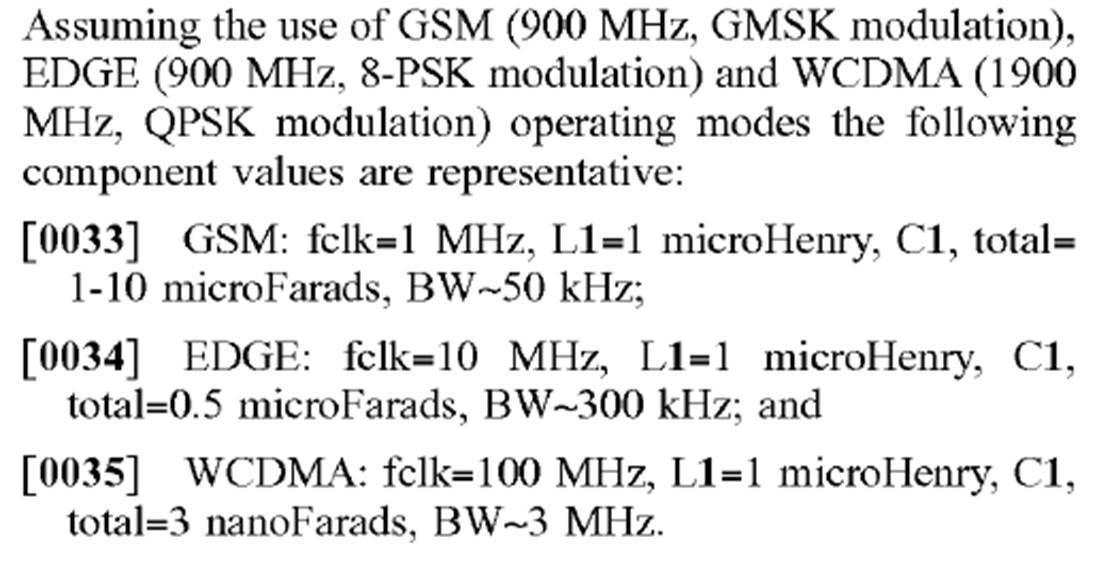
136. Jarvinen explains at [0010] and [0012] that choice of filter components is a compromise, and a fixed filter may be non-optimum. It presents its idea at [0026]:
‘An aspect of this invention provides a low-pass filter having a bandwidth that is variable according to the modulation bandwidth.’
137. This is achieved in Jarvinen with a power supply having a variable bandwidth low pass filter. Crols 2 at 7.57 reproduces its figure 3, with a red arrow denoting the “power supply signal”. So filtering is “during” generation of the power supply signal.
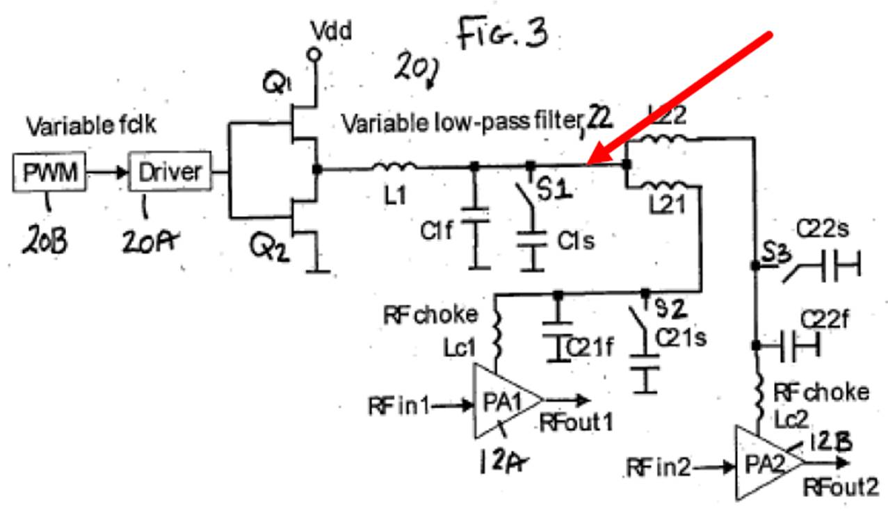
138. The variable bandwidth is achieved with a switchable capacitor C1s in parallel with the fixed C1f (compare Patent in suit Fig.8). Jarvinen also provides a controller to operate this and other switches (see [0039] and Fig.4) depending on the mode.”
179. Oppo said that the opening sentence of [0026] quoted above is the same concept as the Patent. I disagree. The statement is an extremely broad one made in the context where the modulation bandwidth changes when and because a mobile switches modes, a quite different thing from the dynamic change of bandwidth with allocation of resource blocks within LTE. But this was to some extent a rhetorical flourish by Oppo (albeit one that revealed some hindsight): Oppo made a concrete case that it would be obvious to modify Jarvinen and implement it in LTE, making the variable filter in Figure 3 such that its cut off frequency was varied based on resource block usage by the mobile.
Pozzoli 2 and 3
180. Working from the claim charts provided by Oppo and my decisions as to claim scope, the differences between Jarvinen and claim 1 are:
i) Feature 1[b]: there is no use of resource blocks in Jarvinen.
ii) Feature 1[e]: Jarvinen has a variable bandwidth low pass filter but it is not varied according to resource blocks.
Pozzoli 4, assessment
181. Oppo’s case is that it would be obvious to use Jarvinen in LTE; that based on the CGK about varying resource blocks in the standard it would be obvious to vary a filter’s bandwidth in dependence on the number being used. If accepted, this would deal with features 1[b] and 1[e] together.
182. The main planks of this case were that:
i) Jarvinen has a variable bandwidth low pass filter.
ii) Jarvinen teaches that that has an advantage (at [0010] and [0012]).
iii) It was agreed CGK (see paragraphs 37 and 38 of the ASCGK) to vary a filter in accordance with bandwidth.
iv) The use of variable RBs in LTE.
v) The 1 RB v 100 RB point.
183. Oppo said that it would be obvious to have such a variable filter:
i) Of the LC type actually shown in Jarvinen at the output of a pure SMPS.
ii) In the form of a hybrid power supply “e.g. Wang, Kwak” incorporating variable bandwidth LPFs somewhere, it being obvious to do some simulations on them.
iii) Of the Reynaert type with a “splitter” filter.
184. On my interpretation of claim 1, the LC filter shown in Jarvinen already satisfies claim feature 1[d]. Consideration of the other possibilities I have just mentioned arises (a) in case I were wrong about claim interpretation, and (b) in any event to meet Nokia’s arguments that the LC arrangement in Jarvinen would be rejected by the skilled team as unsuitable for the wide bandwidth of LTE.
185. Nokia’s main contentions were (I have aimed to transpose them from the way they were put in relation to Arayashiki, for reasons explained above, and they somewhat overlap):
i) Jarvinen uses its LPF for a different purpose, namely multimode phones.
ii) Jarvinen is about a problem with an SMPS and would have been “old news” for a skilled team considering LTE with its wider bandwidth.
iii) The whole idea of using an SMPS had been overtaken in this context by Wang.
iv) Using an LC filter at the output of an SMPS had the concrete problem of dissipating power undesirably.
v) The notion of doing simulations without a clear goal or expectations was not a sound basis for obviousness.
vi) The 1 RB v 100 RB point was bad on the facts.
vii) Reynaert was not CGK and using it as suggested was not put to Prof Nauta.
viii) The idea of “other filters” had not been adequately developed.
186. I agree with Nokia. It had much the better of all these arguments. Oppo’s starting point for all of this was the idea that LTE was going to require a variable bandwidth filter because of the variable usage of RBs. That in turn was founded on the 1 RB v 100 RB point which I have rejected. So the argument is built on sand. Oppo’s case needs a conceptual leap in this respect which requires looking at Jarvinen in much more abstract way than the skilled team would do. This can be seen in the way that Oppo read [0026] of Jarvinen and in the way it also built its case around paragraphs 37 and 38 of the ASCGK as “soundbites” and which do not in any event say what Oppo claims (they are not general CGK principles that one should always adjust the bandwidth of variable LPFs for the current bandwidth).
187. I also agree with Nokia that the skilled team would think that an SMPS of the kind in Jarvinen was unlikely to be relevant or useful in LTE. They would know that LTE was to have a much wider bandwidth than the standards mentioned in Jarvinen. If they did carry it forward the CGK route would be Wang, which would not have an LPF.
188. Turning to the specific implementation points:
i) I reject the notion of modifying Jarvinen along lines arising from Reynaert since I have found that Reynaert was not CGK.
ii) Arguing that a hybrid power supply “e.g. Wang, Kwak” would be used was much too vague and unconvincing, and it lumped different things together. Furthermore, it showed all the signs of being improvisation necessitated by the course of the trial which had not been properly explored. For example, reliance was placed in closing on what was said to be an LC filter in Kwak in a figure (29.1.4) which had not been explored in evidence at all.
iii) Reliance on unspecified simulations with no clear direction is not a foundation for obviousness. It is too vague and uncertain.
189. Having regard to all these points and in the context of them, I found Prof Nauta significantly more convincing than Dr Crols, especially in the cogency, concreteness and detail of the reasons that he gave.
190. I therefore reject the argument over Jarvinen. I do so on my construction of claim 1 (as contended for by Oppo and relatively more favourable to it) that an LC filter at the output of a pure SMPS could satisfy feature 1[d] of the claim.
191. This means that amendment B to the claims is not necessary, but for reasons given above it would also not be obvious to move from Jarvinen to a different LPF set-up as contended for by Oppo.
Hadjichristos
192. Hadjichristos is an Ericsson article from 2004. It was published on the IEEE website. Its title is “A Highly Integrated Quad Band Low EVM Polar Modulation Transmitter for GSM/EDGE Applications”.
193. The transmitter it discloses is quad band because it works for GSM and EDGE, and at two frequencies for each.
194. I accept that the skilled team would expect that the publication was a strong one given its pedigree and given that it relates to a real design, but that does not in itself mean that they would think it was relevant to LTE.
195. Oppo relies on Figure 2 and Figure 3.
196.
Figure 2 is as follows:
197. This is how the reader would see Figure 2. Oppo relies really only on part of it, and I take the following blown-up and coloured section from Oppo’s opening skeleton argument:

198. The yellow is the DAC, the green is an LPF and the red is a linear power supply on a separate IC (the blue is not relevant to the main arguments at trial; Nokia sought to make something of it but I find that there was no effective challenge to Dr Crols’ evidence that it just amplifies the input).
199. Figure 3 shows circuitry permitting programmatic adjustment of the LPF. The reason for the adjustment in Hadjichristos is to compensate for manufacturing process variations, as was CGK. Oppo accepted that because GSM and EDGE had fixed bandwidth there would be no need to adjust the LPF bandwidth in normal operation.
200. Oppo relied in particular on the following text from page 1:
“Critical parameters are … Phase and amplitude bandwidth (BW) as it directly affects the design of the BB low pass filters, the transmit PLL loop BW and the BW of the CMOS PA controller. The minimum required BW for the amplitude and phase parts is approximately twice the symbol rate, which for EDGE is 270.833 ksps.”
Pozzoli 2 and 3
201. Working once more from the claim charts:
i) Feature 1[b] is absent because Hadjichristos is not for LTE and so there is no use of resource blocks.
ii) Feature 1[d] is disputed because Oppo said the green LPF is “integrated” with the power supply and Nokia said it was not.
iii) Feature 1[e] is missing because although the LPF is programmably adjustable, its adjustment is not dependent on resource blocks.
Pozzoli 4, assessment
202. Because Hadjichristos has an LPF after the DAC and prior to the power supply, there are fewer complexities over its implementation, or changing its implementation, than with Jarvinen.
203. The central issue is however similar: whether it was obvious to make the conceptual leap so as to take an LPF in a product for a different standard which was there for a different purpose (dealing with production variation) and use it for a different purpose in LTE.
204. I make this comparison with Jarvinen not because the two documents can be read together - they of course cannot - but just so that I can be briefer by referring back as appropriate.
205. In its claim chart, Oppo suggested that the passage from page 1 quoted above “teaches that the filter BW should be tailored to signal BW” and it referred again to paragraphs 37 and 38 of the ASCGK. This is another instance of generalising out the teaching and then artificially bending it back towards the specifics of LTE. The statement is too general to point to anything concrete of relevance. I reject the reliance on the ASCGK for the same reasons as above in relation to Jarvinen.
206. Apart from that, the argument again relied on the 1 RB v 100 RB point that I have rejected and the conceptual jump to using a variable filter because the variable RBs in LTE would call for it. This is even weaker than in relation to Jarvinen, though, because the purpose of the LPF being variable in Hadjichristos is merely the CGK one of dealing with production variation and is unrelated to the fact that the transmitter changes from one fixed bandwidth to another from time to time. It is no answer to this to say that Hadjichristos is a good paper which presents a real product; it is, but it is just directed to something else.
207. Nokia made the following further points:
i) It was artificial to focus on something that was CGK (LPF adjustment for production variation). The skilled team’s attention would not be caught by it. There is some force in this but I also accept Oppo’s point that obviousness can arise from a statement of something banal.
ii) Hadjichristos may have been an interesting achievement for its time but GSM/EDGE solutions were not of interest in deciding what to do in an LTE context.
iii) Oppo’s focus on the parts of Figure 2 referred to above was artificial and selective, coming from hindsight.
iv) The same point about modelling/simulations as applied to Jarvinen and which I accept for the same reasons.
208. Points i) to iii) go together and merit a little more comment. As I say, I agree with Oppo that a patentee cannot just sideline prior art because, or to the extent, that it is unspectacular. It is not only possible to have obviousness over accepted things, but positively important to protect the public from finding that patents block the routine development of the everyday. But there is more to it than that when the attack over a piece of prior art involves focusing in on some specific part of a larger scheme. It is relevant to ask whether and why they would do that. Dr Crols’ evidence was that the skilled team would be looking for “new architectural points” in Hadjichristos and this seemed to be the justification for focusing in on the aspects Oppo relied on, but it was inconsistent with the fact that the variable LPF to cope with production variations was CGK. This was another area where Dr Crols’ reasons were not convincing.
209. Point ii) is part of this picture and I agree that Prof Nauta’s concrete reasons why carrying GSM/EDGE implementation across to LTE would not have been natural were strong, and not really challenged (see paragraphs 138(e) to (g) of his first report in particular).
210. So I reject the attack of obviousness over Hadjichristos. It simply would not have been obvious to take just part of it and redeploy it in LTE for a different purpose; nor, given my rejection of the 1 RB v 100 RB point, would it have been in the skilled team’s mind to change the filter bandwidth dynamically with RB usage of an LTE mobile.
211. I record that Prof Nauta made some detailed points about implementation difficulties with Hadjichristos that might dissuade the skilled team from taking it forward even if they had had the basic idea of the Patent. I did not find them convincing and anyway they sat ill with Nokia’s assurance that it was not attacking the enablement of the prior art.
212. Given my decision on the above points it does not matter whether the LPF in Hadjichristos is “integrated”, but I would have found that it is not, given the separation of the LPF from the power supply by multiple intervening components with different functions.
Claim 6
213. In dealing with claim interpretation I have held that the “feed-forward” requirement of claim 6 needs more than merely a signal from input to output.
214. The situation on the evidence is an odd one in that neither side really cross-examined to whether claim 6 was independently inventive. Dr Crols said that both feed-forward and feedback were well known options for applying a correction. Prof Nauta gave reasons more specific to the individual citations about why feed-forward would not be obvious (Hadjichristos at paragraph 393 of his first report, Jarvinen at paragraph 403).
215. I do not think it is desirable to decide this issue purely on the basis that there was no cross-examination. Claim 6 was a minor issue and there was time pressure at trial. Neither side is treated unfairly as a result of there being no cross-examination because each expert knew what the other said and had a chance to respond even if they did not take it: see Edwards Lifesciences v Boston Scientific [2018] EWCA Civ 673 [62]-[70]. I also was not addressed in argument about how to proceed when neither side’s expert was cross-examined.
216. I accept Dr Crols’ general if rather abstract evidence that feed-forward was an obvious way to apply a correction if one were needed. But:
i) As to Jarvinen I also accept Prof Nauta’s evidence that the LC filter is necessary at the output of the SMPS. There is no sensible way to relocate it to a feed-forward path of the SMPS. Had Oppo satisfied me that it was obvious to have an LPF earlier in the circuit then I might have accepted that using feed-forward would be obvious, but it did not do so.
ii) As to Hadjichristos, I have held that the LPF is not “integrated” into the SMPS. Prof Nauta said that the LPF in Hadjichristos was associated with the sigma-delta convertor and it would not be obvious to move it. I found this convincing. Since the LPF is substantially separated from the SMPS it cannot be on a feed-forward path of it.
217. All this being so I reject the attack on claim 6, but my reasoning springs really largely from what I have already said on claim 1.
218. I note also that Oppo submitted that claim 6 makes no technical contribution. I disagree since it provides a correction in a specific way where one is needed.
Sufficiency squeeze
219. I have commented on this above and it is picked up where it might bite. It has done its job and constrained Nokia in what it has been able to say on obviousness but it does not have separate significance beyond that.
Amendment
220. I have to consider Amendment A and Amendment B.
221. Amendment A is to add a statement that Figure 3 is not claimed and so to bolster Nokia’s position on the “integrated” aspect of the dispute on the interpretation of claim feature 1[d] and thereby ensure the LC filter in Jarvinen cannot satisfy the feature. It is sought unconditionally in the sense that Nokia will implement it even if it is not necessary for validity, but it does not accept that there is invalidity without it.
222. Oppo opposes it because it says that it lacks clarity and adds matter.
223. Nokia retorts that it is already clear what “integrated” means and that Figure 3 is therefore not within the claims, and it says that tidying up to say that an embodiment is not claimed improves clarity (it supports this with reference to the EPO Guidelines for Examination). It says that there cannot be added matter because the concept of “integrated” was there all along.
224. Amendment B is to add the requirement that the LPF comprises at least one resistor and one capacitor. This is a cumbersome way of saying it must be an RC filter and so directly excludes Jarvinen’s LC filter. Oppo says this adds matter because it is an intermediate generalisation from Figure 8. Oppo also made a point about clarity but it was not pursued.
The law
225. The law on clarity is that perfect clarity is not required; it is necessary to be as clear as the subject matter reasonably admits of: LG Philips v Tatung [2006] EWCA Civ 1774.
226. The law on added matter is well known and was not in dispute. A strict comparison must be made and if the amended patent discloses new matter relevant to the invention that was not clearly and unambiguously disclosed before, the amendment is not allowable. A species of this general rule arises when there is intermediate generalisation by taking a feature from a specific embodiment and introducing it into a claim when there is no indication that it was generally applicable. See Nokia v IPCom [2012] EWCA Civ 567.
227. Strictly the comparison is with the application as filed but for present purposes one can look at the granted Patent and that is what both parties did.
228. The UKIPO considered the amendments proposed by Nokia and provided comments on them, saying they were allowable for the reasons given by Nokia. This is always of assistance to the Court and I am grateful for it, but it must be borne in mind that the Office operates under pressure of work and without the significant time and extensive assistance from written and oral submissions that I have had. It is also unfortunately not clear that the UKIPO saw Oppo’s Grounds of Opposition to the amendments prior to commenting.
Amendment A
229. I have held that “integrated” is not a very clear term to begin with. My reasoning on claim interpretation also has the consequence that Figure 3 is not necessarily outside claim 1 - it might or might not be depending on how it was implemented.
230. As a result, Amendment A is not of the benign kind identified in the EPO Guidelines where it is clear that an embodiment is outside the claims but the specification has not been conformed to expressly say so.
231. That being so, I think that the amendment is not sufficiently clear. The skilled reader would not understand why Figure 3 was outside the claims and this would cause further avoidable confusion about the circuit in Figure 3, the “integrated” requirement of the claims, and the relationship of the one to the other.
232. I also think there is at least the danger of a subtle kind of added matter by tweaking the meaning of the concept of “integrated”, a claim feature which is relied on for inventive step by Nokia, as against Jarvinen in particular. This is not just a change of claim scope, which of course in itself does not mean there is necessarily added matter, but of presenting a slightly different invention. However, since I reject this amendment for lack of clarity and since the amendment is not needed anyway, I prefer not to express a concluded view.
Amendment B
233. There is no express basis for Amendment B. There is also no express basis for the concept of an RC filter,
234. Nokia relied on Figure 8, which is a preferred embodiment. However, it has other features beside the one resistor and one capacitor referred to in the proposed amended claim. Crucially, and by way of example as well, it has two capacitors and would not work without them both. So the amendment seeks to take just a subset of a collection of features, which collection is together necessary together for the operation of the embodiment. I consider that that adds matter.
235. The reality, as I have foreshadowed, is that Nokia wanted to limit the claims to RC filters without having basis for it. Counsel for Nokia met this by arguing that RC filters were known. So they were, and indeed they were CGK, but it has never been enough on its own to justify adding a claim feature that it was CGK. That would be almost the same as saying that the test for added matter is the same as that for obviousness, which is of course not the case.
Conclusions
236. My conclusions are:
i) The Patent is valid as granted.
ii) The Oppo mobile phones in issue infringe claim 1 of the Patent with the software that they had prior to the Update, but not claim 6.
iii) I would not allow either amendment to the Patent.
237. For the sake of clarity as to the scope of these findings, I reiterate that (a) Nokia has accepted that the Oppo mobile phones in issue do not infringe with the software post-Update, and (b) I have made no finding about the situation with other mobile phones and in particular Nokia’s assertion that more recent models have not received the Update is yet to be determined.
238. I will hear Counsel as to the form of Order if it cannot be agreed. I direct that time for seeking permission to appeal shall not run until after the hearing on the form of Order (or the making of such Order if it is agreed). I draw attention to paragraph 19.1 of the Patents Court Guide, which says that a hearing on the form of Order should take place within 28 days of hand down. In the present case, 28 days from hand down will be 7 December 2022. It would be preferable to deal with all issues then, but I recognise that addressing the point about the state of more recent models and Oppo’s willingness and ability to ensure the Update is applied may not be ready to be determined then. I encourage the parties to liaise about this and to consider whether consequential matters might be heard in two stages. For guidance, I cannot see presently any reason why any applications for permission to appeal, confidentiality, and costs cannot be dealt with within 28 days.
SCHEDULE TO JUDGMENT - “ASCGK”
Claim No: HP-2021-000023
IN THE HIGH COURT OF JUSTICE
BUSINESS AND PROPERTY COURTS OF ENGLAND AND WALES
INTELLECTUAL PROPERTY LIST (Ch)
PATENTS COURT
BETWEEN
NOKIA TECHNOLOGIES OY
(a company incorporated under the laws of Finland)
Claimant
and
(1) ONEPLUS TECHNOLOGY (SHENZHEN) CO., LTD
(a company incorporated under the laws of the People’s Republic of China)
(2) UNUMPLUS LIMITED (t/a OnePlus)
(3) GUANGDONG OPPO MOBILE TELECOMMUNICATIONS CORP, LTD
(a company incorporated under the laws of the People’s Republic of China)
(4) OPPO MOBILE UK LTD
Defendants
STATEMENT OF AGREED COMMON GENERAL KNOWLEDGE
1. Radio Transmission
1. In a mobile phone network, the baseband circuitry of the mobile phone (or base station) produces signals which need to be transmitted over-the-air to the base station (or mobile phone). (Crols 1 §6.8)
2. Through a process called "modulation", these baseband signals are encoded onto a carrier wave by changing the frequency, phase and/or amplitude of the carrier wave. More precisely, a modulator (in the baseband, and/or the radio transmitter front-end) will receive the incoming bits of data (e.g. 1s and 0s) and, using a pre-defined modulation scheme, compute digital "symbols" from specific combinations of 1s and 0s. These symbols set the frequency, phase and/or amplitude characteristics of the outgoing radio wave. (Crols 1 §6.9; Nauta 1 §32)
3. Wireless transceivers transmit and receive information (such as voice and data) using radio frequency (RF) signals. Transmitters operate by amplifying weaker signals. In order to amplify a signal for transmission by an antenna additional energy needs to be added from a supply of electrical energy. (Nauta 1 §§30 & 33; Crols 1 §§6.13 and 6.15)
4. Desirable characteristics of radio transmitters, and their amplifiers, included (Crols 1 §6.13):
a) Linearity - that is, the transmitter produces a power amplified version of the original signal with minimal distortion to its phase and amplitude (if the modulation system is not a constant envelope one); and
b) Efficiency - that is, the power amplified version is produced without the transmitter dissipating too much power itself.
5. The RF frequency band of a radio interface may be subdivided into a number of "channels" which are used for conveying information signals. The difference in frequency between the centre of one channel and the centre of an adjacent channel is known as the "channel spacing". The term "bandwidth" is a measure of the width of a frequency range (measured in hertz (Hz)), for example a channel bandwidth or a frequency band bandwidth. (Nauta 1 §188)
1.1 Modulation schemes
6. A carrier wave can be described according to three key characteristics: its amplitude, frequency and phase. Modulation is a process by which one or more of these characteristics is varied based on the information to be transmitted. (Nauta 1 §36)
7. In PSK the phase of the carrier wave is modulated. The phase of the carrier is stepped to certain discrete values, depending on the data to be transmitted. Particular variants include Binary PSK (BPSK), Quadrature PSK (QPSK), 8PSK, and 16 PSK. (Nauta 1 §49)
8. A transmitter that is transmitting a phase modulated signal does not need to have constant amplitude, as there is no information in the amplitude variation of the signal. (However, the amplitude of the signal may decrease in moving between phase values). (Nauta 1 §51)
Gaussian minimum shift keying
9. Minimum shift keying is a type of continuous-phase frequency-shift keying. The frequency shift is proportionate to the bitrate of the signal so that transitions between frequencies do not cause any phase discontinuity (sharp edges between symbol transitions) and the signal has a constant amplitude. It can be amplified by a non-linear amplifier because distortion in the amplitude of the received signal does not affect the received symbol. (Nauta 1 §52 and 54)
10. Gaussian minimum shift keying further involves passing the I and Q digital samples through a digital ‘Gaussian’ filter before application to a frequency modulator. GMSK has narrower phase shift angles compared to MSK, which reduces sideband power, in turn reducing interference with other channels and improving spectral efficiency. GMSK was the modulation scheme chosen for GSM. (Nauta 1 §55)
Quadrature amplitude modulation
11. In quadrature amplitude modulation both amplitude and phase are varied. Higher order QAM modulation features increasing numbers of points on the constellation, for example 64 QAM features an 8 by 8 grid of possible values. (Nauta 1 §56 and 57)
12. The greater the number of values in a constellation the greater the amount of information that can be conveyed by a single symbol. This allows increased data rates at the same symbol rate. If a modulation scheme has more data per symbol it may be referred to as higher-order modulation. (Nauta 1 §58)
Orthogonal frequency division multiplexing
13. In orthogonal frequency division multiplexing (OFDM) there are a number of subcarriers in the frequency domain, each of which is independently modulated with information for transmission. In effect, each of the subcarriers has its own constellation of I and Q data. (Nauta 1 §59)
14. All the subcarriers have the same bandwidth. The centre frequency of each subcarrier is specified relative to the bandwidth of the subcarrier such that subcarriers are orthogonal to their adjacent subcarriers. This means no guard bands are required between the subcarriers and they can all be packed closely together. (Nauta 1 §60)
15. In creating a signal for transmission a digital representation of the signals on all these subcarriers is combined in the digital domain, and converted to analog I and Q signals which are placed onto a carrier wave for transmission. (Nauta 1 §62)
Modulation schemes in use at the Priority Date
16. GSM/GSM EDGE (the so-called 2G and 2.5G standards) used GMSK/8PSK. UMTS (3G) used QPSK. (Nauta 1 §190).
17. Some standards have common elements, such as modulation schemes, which meant that it was possible to try and make more efficient use of space, or reduce the required number of components, by creating transmitters that could work for multiple standards. Transceivers that are compatible with more than one standard are called ‘multimode’. (Nauta 1 §186)
Passive circuit elements
18. This category includes: (Nauta 1 §70)
a) Resistors - which oppose the flow of charge; resistance is measured in Ohms (Ω);
b) Capacitors - which store energy in an electric field; capacitance is measured in Farads (F); and
c)
Inductors - which store energy in a magnetic field; inductance is measured in Henrys (H).
Figure CGK-1: Passive circuit elements and impedance
19. Conventional symbols for each are shown in Figure CGK-1 above. As also there indicated, each passive circuit element is characterised by an impedance, Z. For a capacitor and an inductor this is frequency dependent (because the value w is frequency dependent), but it is fixed for a resistor. A combination of passive components can also be characterised as having an impedance. (Nauta 1 §71)
Active circuit elements
20. Active circuit elements rely on a source of energy and can often inject power into a circuit. A transistor is an example of an active circuit element. Transistors can control the flow of an electric current and are often used as an amplifier or a switch. The current flowing between two of the transistor’s terminals may be controlled by the voltage at a third. (Nauta 1 §72 and see also §73 and §74)
2.1 DACs
21. Where a digital baseband processor is used, the radio transmitter will need one or more digital-to-analog converters, or DACs, to convert the digital baseband signals into an analog/radio signal for transmission. In a polar modulation structure (see section 4 - "Polar Transmitters" below), a DAC will be required on the amplitude and phase paths to convert the digital polar information into an analog amplitude signal and analog phase signal (Crols 1 §6.27).
22. There are different ways of constructing a digital to analog converter. DACs will have a sample rate, which is the rate at which they are outputting the signal. (Nauta 1 §78)
23. DACs are typically referred to as ‘n-bit’, where the DAC has 2n levels of output. For example, a 10-bit DAC would have 1024 different output levels. DACs convert digital information from the baseband into an analog signal using a process known as "sample-and-hold" (or "S/H"). This, however, creates a time-discrete, jagged or staircase-like, output, as shown below right. The difference between the staggered output and the desired smooth analog waveform is called quantization noise, which will need to be removed otherwise it can cause spectral regrowth (see paragraph 72 below). The output is then low-pass filtered to reconstruct an analog signal. (Nauta 1 §79; Crols 1 §6.28)
Figure CGK-2: Illustration of a 6-bit DAC
The sigma-delta converter
24. One method of digital to analog conversion is known as a sigma-delta converter (delta-sigma is also used). A one-bit sigma-delta converter produces a signal with only one of two values: the voltage is either at a minimum value or a maximum value (i.e. it is a 1-bit DAC) and the switch is operated several orders of magnitude faster than the frequency of the desired output signal (e.g. a 1kHz signal may require MHz order switching). All the information is therefore in the timing of the pulses. (Nauta 1 §80)
2.2 Filters
25. A frequency domain filter allows signals within a frequency range to pass and attenuates signals either side of that frequency range. Such filters include (Nauta 1 §90; Crols 1 §6.53):
a. Low Pass Filters (LPF) - which allow signals from 0 Hz (DC) up to a “cut-off frequency” (also referred to as a “corner frequency”) to pass and attenuate signals above that frequency;
b. High Pass Filters (HPF) - which allow signals above a “cut-off frequency” (or “corner frequency”) to pass and attenuate signals below that frequency;
26. Low pass filters (or LPFs) were, at the priority date, a common component used in radio transmitters, and in particular polar modulation structures. (Crols 1 §6.53)
27. A first order low pass filter may be implemented, for example, using a resistor and a capacitor as shown below. The cut-off frequency, fc, for such a filter is given by 1/(2.π.R.C) (where R is the resistance and C is the capacitance). The figure below shows a simple first order low pass filter for a voltage signal in and a voltage signal out (Nauta 1 §91; Crols 1 §6.54)

Figure CGK-3: First order low pass filter
28. A low-pass filter can rely on the frequency dependent behaviour of capacitors. In this circuit the impedance of the capacitor varies inversely with the frequency of the voltage across it. At low frequencies the capacitive impedance of the capacitor will be very large compared to the resistive value of the resistor, R. This means that the voltage potential, VC, across the capacitor will be much larger than the voltage drop, VR, developed across the resistor. At high frequencies the reverse is true with VC being small and VR being large due to the change in the capacitive impedance value. (Nauta 1 §92; Crols 1 §6.54)
29. As the frequency of the input increases the impedance of the capacitor decreases, causing the voltage potential across the capacitor to drop below that of the resistor. That means that above a frequency defined by the relationship between the capacitor and the resistor, i.e. the cut-off frequency 1/(2.π.R.C), the output from the low-pass filter will be attenuated. The extent of this attenuation will increase the greater the frequency. (Nauta 1 §93; Crols 1 §6.54)

Figure CGK-4: Second order low pass filter
30. Filters can be first order, second order, or higher order. The diagram above shows a second order low-pass filter. The figure below shows the frequency-domain amplitude response of two low pass filters; one of first order and one of second order. The cut-off frequency is shown as fc. Signals above this frequency are attenuated. A first order filter has a ‘roll-off’ of 20dB per decade of frequency and a second order filter has a ’roll-off’ of 40dB/dec, i.e. the second order implementation is a “steeper” filter than the first order implementation. This is true regardless of the specific values chosen for the components. (Nauta 1 §94; Crols 1 §§6.59-6.60)
 Figure CGK-5: Frequency-domain amplitude response of first and second order low pass filter
31. In the diagram above the measured response for each filter is shown by the solid red curved line. In each case the asymptotic line is shown as a dotted red line (an asymptotic line is one which approaches the value of the curve, in this case as the frequency increases to infinity). The slope of the asymptotic line shows the order of each filter, and crosses the extrapolated low frequency gain line at the cut-off frequency. (Nauta 1 §95)
32. The extent of filtering that is required is determined by the application. Where a normal DAC might require a second order filter, a sigma-delta converter might require a fifth order filter. It is possible to determine the order of a filter from the effect it has on a signal that is passed through it. (Nauta 1 §96)
33.
A high-pass filter can be achieved by swapping the position of the resistor and the capacitor as follows (for a first-order high-pass filter): (Nauta 1 §97)
Figure CGK-6: First-order high pass filter
34. Both high-pass and low-pass filters cause phase delay in the output signal resulting from the time taken for the capacitor to store its charge. (Nauta 1 §98)
35. Filters can also be created using an inductor L and a capacitor C, as shown below:
Figure CGK-7: Inductor/capacitor low-pass filter
The use of an inductor can reduce losses in the filter design by reducing the amount of power that is dissipated as heat. Inductors also have frequency-dependent behaviour. At high frequencies they have a high impedance but at low frequencies they have a low impedance. (Crols 1 §6.55, Nauta 1 §99)
36. High-pass and low-pass filters can also be ‘active’ (rather than passive) where they include one or more active components, typically an amplifier (Nauta 1 §100, Crols 1 §6.54).
Setting the Corner Frequency of a Low-Pass Filter
37. Whenever a low-pass filter is inserted into a radio transmitter architecture, the Skilled Team has to set an appropriate corner frequency for that filter. (Crols 1 §6.65)
38. The Skilled Team would know that when using an LPF to suppress unwanted noise, there was a balance to be struck when setting the appropriate corner frequency. Relevant considerations are
(a) The corner frequency has to be high enough, to allow the (bandwidth of the) desired incoming signal to pass. If the corner frequency is set too low, and amplitude information is not allowed to pass, data will be lost from the transmitter signal and this will reduce the linearity of the radio transmitter; but
(b) The corner frequency has to be not too high, as this will make it more likely that unwanted high frequency noise will be superimposed on signal being transmitted which can result in unwanted spectral regrowth which can leak into neighbouring frequencies occupied by other users and cause the radio transmitter to fail to satisfy the out-of-band noise and spurious emission requirements set by the standards (see below).
The Skilled Team would choose a suitable corner frequency, taking these considerations into account in the context of the signal being filtered (Crols 1 §6.65; Nauta 2 §32). The parties dispute the extent to which a further consideration would also need to be taken into account - see issue 3 of the List of Disputed Common General Knowledge.
39. An integrated circuit is one in which all the components are formed using a single piece of semiconductor material, mostly silicon. When an integrated circuit is referred to as a CMOS circuit that means that it includes both NMOS and PMOS transistors. A BiCMOS circuit includes NMOS and PMOS transistors, and also bipolar junction transistors (BJTs). (Nauta 1 §75)
40. Integrated circuits can also include other electrical components such as capacitors, resistors and inductors. However, there are limits to the size of the components which can be integrated onto the chip in this way. For example, at the priority date the limit to on-chip inductor size would be of the order of 2 nano Henrys - 10 nano Henrys would be too large. For capacitors 10s of pico Farads could be on chip. Resistors could be up to a few mega Ohms. (Nauta 1 §76)
Process Variations in Integrated Circuits
41. Variations in both resistor and capacitor value in integrated circuits arise as a result of the way in which the components are formed in the production of integrated circuits. This is a problem that is universal to resistors and capacitors which are included in integrated circuits. Variations in the production process for an on-chip RC filter could lead to variations in the cut-off frequency of the filter, which could be +/- 30% (or more) from the desired cut-off frequency. (Crols 1 §6.71; Nauta 2 §34)
42. Counteracting these production process variations reduces the potential for unwanted noise, and so helps the radio transmitter satisfy its spectral mask. (Crols 1 §6.70)
43. It was possible to design integrated circuits to compensate for such production process variation, where it was necessary to do so, by making one or more of the relevant components adjustable.
44. The Skilled Team would also know that this adjustability to compensate for production process variation could be programmed, or pre-set, rather than having to be done manually. The Skilled Team would be able to apply this knowledge to achieve a filter in an integrated circuit having a cut-off frequency which was closer to that desired by adding additional on-chip components that could be switched in or out to tune the filter to be closer to the desired cut-off frequency. (Crols 1 §§6.68-6.79; Nauta 2 §34)
2.4 Amplifier design
45. NMOS transistors can be used in logic circuits where signals are switched between logic 1 (Vdd, the positive power supply) and logic 0 (Vss, the negative power supply or ground). Switches are also used to direct or route signals in a certain direction in an electronic circuit. (Nauta 1 §107)
46. An NMOS transistor can also be used as a voltage controlled current source. A "current source" is a circuit element that forces a current to flow between its two terminals. If the difference between the gate and source voltage (Vgs) is smaller than the threshold voltage (VT) there is no current. If Vgs is larger than VT then the current source forces a current (Id) to flow as shown by the characteristics of graph (iii), shown below. The slope of the line on the graph (iii) is gm: the amperes per volt that are produced by the amplifier. For a limited range of input voltages around the ‘bias point’ this will give rise to an approximately linear relationship between input voltage and output current. This region can also be referred to as a transistor’s saturation region. (Nauta 1 §§109-111)
Figure CGK-8: NMOS transistor acting as voltage controlled current source
47. The above circuit can be described as a (simple kind of) transconductance amplifier: an amplifier which generates an output current from an input voltage. This kind of amplifier can also be called a ‘GM block’, illustrated schematically by a triangle with the end missing. (Nauta 1 §112)
Figure CGK-9: Illustration of GM block
48. A transistor can also be used to create a voltage amplifier. Where the transistor acts as a voltage controlled current source (transconductance amplifier), it can be used to create a larger output voltage than it receives as an input by the addition of an output resistor. The input voltage is “converted” to a current in the NMOS transistor and this current also flows through a load resistor (RL) connected to the positive supply Vdd, creating a voltage drop across it. If Vin increases, Id increases and the current though RL increases and so Vout decreases. The function is therefore an inverting voltage amplifier; the input voltage variation is amplified and changes sign. (Nauta 1 §§115-116)
Figure CGK-10: NMOS transistor acting as inverting voltage amplifier
49. An amplifier can be indicated by a generic triangle symbol with one input and an output, shown below. This schematic representation may be maintained for more complicated arrangements of transistors, including the different classes of amplifier described below. (Nauta 1 §117)
Figure CGK-11: Amplifier symbol
50. An amplifier may also be illustrated as below, with two inputs, two supplies, and one output: (Nauta 1 §118)
Figure CGK-12: Illustration of a voltage amplifier
51. The diagram shows the supply voltage that is applied to the amplifier (Vs) and the signal for amplification at V+ and V-. The output voltage, Vout, is the amplification of the difference between the V+ and V- inputs. If it has very large (effectively infinite) gain it will be an ‘op-amp’ (also known as an ‘operational amplifier’), and feedback can be used to provide a useful output. For example, feedback to the negative input will cause the output signal to increase until the feedback signal is equal to the positive input. As in the case of the transconductance amplifier above, voltage amplifiers will have a linear region. (Nauta 1 §§119-120)
52. Power amplifiers are classified as linear (e.g. classes A, B or AB) or non-linear (e.g. classes C (current dependent), D (voltage dependent) or E (voltage dependent)). Class C amplifiers can be used in a linear and a non-linear way. The details of how these PAs work is not relevant except to say that both have their drawbacks from a linearity-efficiency perspective - in general: (a) linear PAs operate inefficiently at low-medium input power levels, but linearly; and (b) non-linear PAs operate efficiently but not necessarily linearly. (Crols 1 §6.16, Nauta 1 §121 to 124).
53. Class D and S amplifiers may be referred to as switching amplifiers. When used in the power supply of RF power amplifiers they are often called switched-mode power supplies (SMPS) (Nauta 1 §125, Crols 1 §§6.33-6.34).
54. Symbols can be represented in either the in-phase & quadrature form or polar form. In-phase and quadrature form refers to the fact that any outgoing radio wave can be made from a combination of two waves which have the same frequency but are separated in phase by 90 degrees (e.g. a cosine and sine wave). Consequently, points on the outgoing radio wave can be described by their in-phase (I) and quadrature (Q) coordinates which can be plotted as a pair of coordinates on a 2-dimensional graph. A symbol represented by its I/Q coordinates may alternatively be represented, in polar form, by reference to its phase and amplitude. (Crols 1 §6.10; See also Nauta 1 §37 and 38)
55. In a polar transmitter the cartesian I and Q signals are converted into a phase component and an amplitude component. The phase component is directly amplified by a power amplifier (PA), the output power of which is determined by its power supply level Vsupply. The amplitude component is applied to a power supply which is used to generate the power supply signal, and drive the gain, of the PA to restore the amplitude component to the RF signal (Crols 1 §6.18, Nauta 1 §134). Figure 1 of the patent illustrates the overall arrangement.
56. In the amplitude pathway the amplitude part of the signal, also referred to as the signal envelope, is given the appropriate voltage to create a supply voltage which can be applied to the supply input (Vsupply) of the power amplifier. When the power amplifier amplifies the phase modulated phase signal by the varying supply voltage, the signal for transmission is generated. (Nauta 1 §136)
57. There are many variants of this technique. Commonly used terms are ‘Envelope Elimination and Restoration’ (EER) and ‘Envelope Tracking’ (ET). (Nauta 1 §137, Crols 1 §§6.17-6.19)
58. The original EER scheme (devised by Leonard Kahn in 1952) separated the amplitude and phase components in the analog domain using an envelope detector and a limiter but by the priority date these components would typically have been produced digitally in the baseband circuitry. (Crols 1 §6.17 and 6.18)
59. Generating a supply voltage for the power amplifier carries with it some of the same problems involved in creating an efficient power amplifier. The amplitude information needs to be conveyed to the power amplifier with the energy required for transmission. (Nauta 1 §139)
4.1 Linear Power Supply
Figure CGK-13: Linear amplifier used to generate PA supply voltage
60. The above diagram first shows a linear amplifier used to generate a supply voltage for the PA, Vsupply. The input voltage to the linear amplifier (i.e. that from the battery in a mobile phone) will still at most times be in excess of the desired supply voltage output for the PA (i.e. the amplitude component will be lower than its maximum value). This will cause loss. (Nauta 1 §140 and Crols 1 §6.30)
61. The second diagram above shows a practical implementation, where a large transistor is controlled by a smaller amplifier, such that the output voltage is related to the signal at the gate of the transistor controlled by the smaller amplifier. However, there is still a voltage drop across the transistor which causes loss. (Nauta 1 §141 and Crols 1 §6.30)
4.2 Switched-Mode Power Supply
62. A further alternative is a switched mode power supply or SMPS, pictured below. (Nauta 1 §142) These use a Class D or S amplifier (see Crols 1 §§6.33-6.37; Nauta §125-129).

Figure CGK-14: Switched mode power supply
63. The SMPS uses switches and so has very low loss. While the PA has to operate at radio frequency the power supply for the PA only has to operate at a multiple of the rate of change of the amplitude signal. (Nauta 1 §143)
64. In a switching amplifier, the switching duty cycle expresses for a given period of time how long the incoming voltage VDD is switched on by the amplifier. The higher the duty cycle, the higher the average output power of the SMPS, as shown by the diagram below (where VDD is shown to be 5V): (Crols 1 §6.35, Nauta 1 §126)
Figure CGK-15: Illustration of different duty cycles
65. As shown above, the output of the switches varies significantly, either providing a voltage of 0 volts or the maximum VDD volts. Because of the large variations in power, this signal at this point cannot be used as a power supply signal. An LC low-pass filter therefore needs to be included in the SMPS after the switches to convert these pulses into a smoothed power supply signal which can be received by the PA. The Skilled Team would regard this LC filter as an essential part of the SMPS itself. The amplitude of the signal at the output, the supply voltage, is determined by the duty cycle of the SMPS (i.e. how often the switches are on or off). (Crols 1 §6.36, Nauta 1 §§142-147)
66. The filter at the output is an inductor/capacitor low-pass filter rather than a resistor/capacitor low-pass filter, in order to avoid loss due to the large currents that would otherwise flow through the resistor. The inductor required for this application is too large to be included on-chip as it has to store a lot of energy. The filter smooths out the square wave output from the switches and also reduces the noise from the switching operation by letting through only the lower frequency supply signal (i.e. it is a low-pass filter). (Nauta 1 §146)
4.3 Combination of linear and switching power supply
67. In the period leading up the priority date there had been developments in power supplies for polar transmitters. These involved the combination of linear and switching power supplies to create hybrid arrangements. (Nauta 1 §149, Crols 1 §6.38 and §6.48)
Series combination of linear and switching power supply
68. A series combination of a switching and linear amplifier allows the output from the SMPS to be cleaned up by the linear amplifier, which reduces the voltage drop and the losses compared to a power supply formed of a linear amplifier on its own. (Nauta 1 §150)
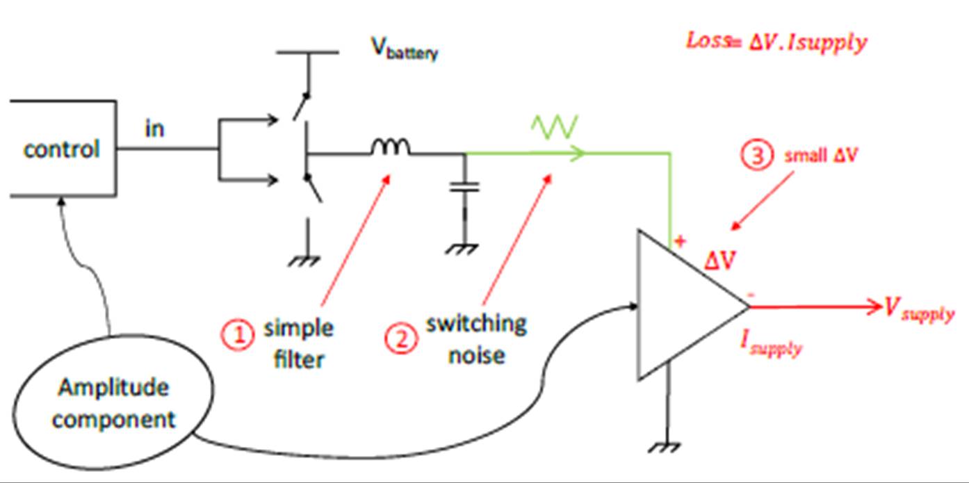
Figure CGK-16: Series combination of switching and linear power supply
69. Amplitude data is used to control the switching power supply, top left. The output from this switching power supply is shown below in black. The output from the switching power supply is fed through a low-pass filter which leads to the output shown in green. This is then provided to the supply of the linear amplifier, which uses that green supply to provide the red Vsupply output for the PA, shown below. The voltage supply to the linear amplifier is closer to the desired output than if the linear amplifier were supplied directly by the battery, and so losses are reduced. (Nauta 1 §151)
 Figure CGK-17: Generation of Vsupply for PA
70. However, if the voltage from the switching power supply drops too low the linear amplifier cannot supply enough voltage to compensate. There is therefore a need for safety margins, and so a large enough voltage drop needs to be engineered across the linear amplifier to protect against this outcome. This limits the efficiency gains that can be made using this arrangement, as the greater the safety margin the greater the power loss in normal operation. (Nauta 1 §152)
Parallel combination of linear and switching power supply
72. Noise and spurious signals lead to errors in received data and reduce the overall capacity of the wireless communication system. Noise and spurious signals can be a result of the environment in which the signal is received, or it can be an unwanted part of the signal that is transmitted. An ideal transmitter would produce only the signal for transmission, but in reality this is not practical. (Nauta 1 §159)
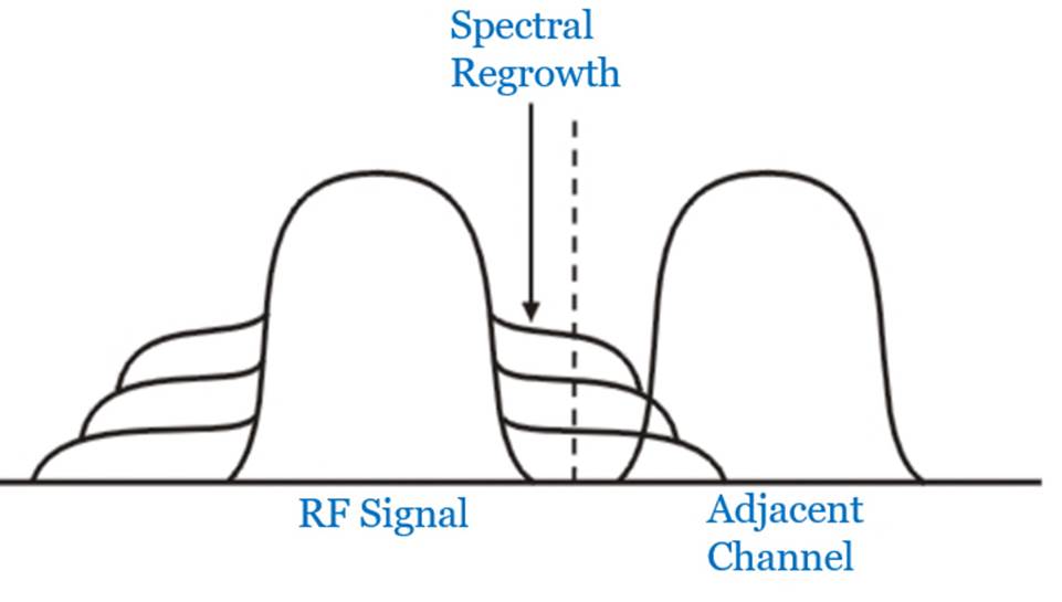
Figure CGK-18: Spectral Regrowth
74. Noise and spurious signals are introduced to the signals in the transmission chain by the operation of the electrical components. There are many different types of noise, and different ways of describing noise which depend on whether it is being discussed in the time domain or the frequency domain. (Nauta 1 §160 to 168; Crols 1 §6.23)
75. There are various different types of noise which are created in polar modulation structures and which can cause spectral regrowth, including quantization noise caused by the DAC and switching noise where a SMPS is used (Crols 1 §6.23):
76. In the early 2000s, radio transmitter designers were finding ways to improve the linearity and efficiency of polar modulation architectures, and limit the noise and spectral regrowth that could be created by these structures (Crols 1 §6.24). If noise produced by e.g., the DAC in the examples above is not reduced, for example by being low-pass filtered, then they have the potential to:
a) increase the amplitude error aspect of EVM (see below) such that the wrong symbol could be received by the receiver; and
b) increase spectral regrowth, which in turn increases the ACLR and spurious emissions. (Crols 2 §5.32).
77. At the priority date it would be usual to position an RC low-pass filter after a digital to analog converter (a) to reduce the sharp-edged output of the DAC and to remove high frequency DAC noise, and (b) to reconstruct the analog signal (Crols 1 §6.62, Crols 2 §5.28). As explained earlier, it would also be necessary to position an LC low-pass filter after the switches in an SMPS when used alone (a) to reduce switching noise and (b) to smooth-out the signal (Crols 1 §6.63, Crols 2 §5.29). Without that, there is no smoothed (usable) power supply output from the SMPS.
6 Transmitter Design Considerations
78. In designing a transmitter there are four particularly important performance requirements: (Nauta 1 §169, Crols 1 §5.10, Crols 2 §§5.31-5.33)
a. EVM, or error vector magnitude;
b. ACLR, or adjacent channel leakage ratio (there are also spurious emissions that are further away than the adjacent channels, which are also important);
c. Output power levels; and
d. Power efficiency.
79. These requirements would be defined by the standard that the transmitter was to be used for (Nauta 1 §191, Crols 2 §§5.45-5.47).
80. A number of secondary considerations are also relevant, including matters such as cost, ease of manufacture, and size. (Nauta 1 §171)
Error vector magnitude
81. Error vector magnitude is a measurement of modulation performance, namely of the difference between the point on the constellation that should be transmitted and that which is actually transmitted. A high error vector magnitude may lead to the wrong symbol being received. (Nauta 1 §172)
82. As the number of points on a constellation increases the margin for error in transmission decreases. If the phase or the amplitude of the signal diverges too far from the constellation point at the receiver, the incorrect value will be recorded when the digital data is re-assembled (subject to any error correction mechanisms) in a receiver. (Nauta 1 §173)
83.
The ‘vector’ part of the term refers to the vector on the constellation between the ideal value and the actual value. This can be displayed graphically. (Nauta 1 §174)
Figure CGK-19: Illustration of Error Vector Magnitude
84. As error vector magnitude grows, the points of the constellation become harder to distinguish. The error vector has both a phase aspect and an amplitude aspect. (Nauta 1 §175)
85. There are a number of causes of high error vector magnitude. One cause is poor linearity in the amplifier. This will tend to cause amplitude error. Higher order modulation schemes have a higher demand for linearity, as there are a large number of possible amplitude values. In contrast, in a modulation scheme such as GMSK there is only a need for phase accuracy, as there is no information in the signal amplitude (this means that GMSK can be amplified with a non-linear amplifier). (Nauta 1 §176)
ACLR
86. Adjacent channel leakage ratio (ACLR), or adjacent channel power ratio (ACPR), are terms which relate to the measurement of the power of the signal in the transmission channel relative to the power of the signal in the adjacent channels. It provides a measurement of the potential interference in the frequency domain that one transmission will cause with another transmission. A further similar term is ACLP, which is the absolute channel leakage power. (Nauta 1 §177)
87.
This leakage can be shown graphically by a frequency domain plot such as the following: (Nauta 1 §178)
Figure CGK-20: Illustration of ACLR
88. Different limits on ACLR or ACPR are specified in different standards. These can be assessed by use of a ‘spectrum mask’, which indicates the acceptable level of leakage graphically on a frequency plot. (Nauta 1 §179)
Output power levels
89. The most critical requirement is the maximum power to be delivered, but it is also necessary to know the steps in power that are required. (Nauta 1 §180)
Power efficiency
90. Power efficiency is important for transmitters for use in mobile devices. At a broad level, the efficiency of an RF amplifier is the amount of the electrical energy that is converted to electromagnetic radiation. A higher efficiency amplifier will reduce the energy consumption of the device when making transmissions at any given power level. (Nauta 1 §181)
91. Losses are caused by the electrical components used to create the amplifier. Electrical resistance causes loss, and the power loss in watts is equal to the resistance of the component in ohms multiplied by current in amps, squared. Power lost in this way is dissipated as heat. (Nauta 1 §182)
92. Different standards will have a different peak-to-average power ratio, or PAPR. The PAPR is determined by the difference between the maximum transmission signal amplitude and the average amplitude. The necessary maximum power sets the requirement for the peak power of the transmitter, but the average power determines which part of the transmitter’s range it will spend the most time operating in. This has important consequences for transmitter efficiency. As a general rule, standards which have amplitude modulation will have a higher PAPR than ones that do not, because the signal amplitude is reduced relative to its maximum amplitude in order to convey information. (Nauta 1 §183; Crols 1 §6.14)
93. At the priority date transmitters would be specifically designed for particular standards and would be required to meet the relevant performance requirements in order to be marketed as being compliant with those standards. (Nauta 1 §184, Crols 2 §5.43)
94. The design brief for a transmitter would include transmitter performance requirements - such as the required transmission frequencies and bandwidths, output power levels, modulation (including both modulation scheme and EVM) and channel leakage (e.g. ACLR) performance requirements - that would be informed by the requirements of the standard that the transmitter was to be used for. The standard would specify both the required performance and how performance is to be tested. (Nauta 1 §191, Crols 2 §5.45-5.47)
95. The LTE standard was still under development in December 2007. Not all of the transmitter performance requirements had been standardised. It had been decided that LTE would use OFDMA in the downlink and SC-FDMA in the uplink, with QPSK, 16QAM and (for the uplink, eventually) 64QAM modulation schemes, which would require a transmitter with high modulation accuracy (and therefore low EVM - for example it was likely that 12.5% would be required for 16QAM) and high PAPR. There were to be a number of different transmission bands at different carrier frequencies, with different bandwidths, including 5, 10, 15 and 20 MHz (a substantial increase over the 3.84 MHz bandwidth of WCDMA). The maximum output power requirements were likely to be in the range of +25 to +27 dBm (i.e. about 0.5 W). The ACLR requirements would depend on the bandwidth of the transmission band, but for a 20 MHz bandwidth it was likely that the requirement would be for a -30 dB difference between the power in the central 18 MHz of the transmission band and the power in the 25 MHz above or below the transmission band. (Nauta 1 §192, Crols 2 §5.49)
96. In LTE a resource block is the smallest unit of physical resources. The bandwidth of a single RB is 180kHz, made up of 12 subcarriers (each with a bandwidth of 15 kHz) in the frequency domain and 1 slot (0.5 ms) in the time domain. (Nauta 1 §193; Crols 1 §6.86)
